Relay question.

nick12ab

Senior Member
Welcome to the club. LOL

"negative" as in (ie) -5V or do you mean 0V?
Yes, a minus voltage.

That would be correct nick, and is one of the reasons why most PNP switches are on the high side where full conduction is easy.

As drawn, with the base at 0v the transistor is "almost" fully on, but still in the linear region and will have to dissipate more heat than is necessary. IT need to go about to about -.7v to saturate. High side switching with a PNP does not have this problem.
Thank you for the clarification.
 

EricD

Member
@ Eric, before I forget (again) best wishes for a speedy recovery. While surgery isn't something to look forward to, we come away from it better off than going in. So again, best wishes for a speedy recovery.

Ron
Thanks Ron, hopefully I'll have done soon so that I can be back on my feet by summer. Not that we get proper summers here in the UK but at least it's warm enough so that I can do some work in the garage.
 

Dippy

Moderator
Don't worry about blunt comments.
Mainly it's because we get so many requests which require teeth-pulling and it's tempting to tar everyone with a similar brush.
There's a thread going right now where the OP hasn't the time to post a schematic - yet, potentially, the problem could be sorted 30 seconds after a schematic appears. The assumption that all other contributors have plenty of time (and have a crystal ball) sometimes causes people here to get a bit peed off. :(
So please forgive the brusqueness.


Back to the plot...
I don't know whether or not the opto is needed really for same reasons as Martin says... i.e. depends on power wiring.


I'm not a Darlington fan; for some devices they drop too much voltage. (Vce).
A small relay can be driven directly by an NPN instead of the Darlington. Much less Vce and therefore more likely to drive relay on better.
PICAXE O/P --- 470R --- NPN(base).

Go to a place like Farnell or RS and do a parametric search for transistors.
I don't know what relay you are using so can't make a suggestion, but for a small 'typical' relay then nearly any old 200mA / 300mA NPN will do. You'll have to check your relay coil spec. first.
 

EricD

Member
Don't worry about blunt comments.
Mainly it's because we get so many requests which require teeth-pulling and it's tempting to tar everyone with a similar brush.
There's a thread going right now where the OP hasn't the time to post a schematic - yet, potentially, the problem could be sorted 30 seconds after a schematic appears. The assumption that all other contributors have plenty of time (and have a crystal ball) sometimes causes people here to get a bit peed off. :(
So please forgive the brusqueness.
Forgiven and forgotten Dippy. I have learned a valuable lessen though, hopefully it'll help keep me out of trouble in the future. LOL


Back to the plot...
I don't know whether or not the opto is needed really for same reasons as Martin says... i.e. depends on power wiring.

I'm not a Darlington fan; for some devices they drop too much voltage. (Vce).
A small relay can be driven directly by an NPN instead of the Darlington. Much less Vce and therefore more likely to drive relay on better.
PICAXE O/P --- 470R --- NPN(base).

Go to a place like Farnell or RS and do a parametric search for transistors.
I don't know what relay you are using so can't make a suggestion, but for a small 'typical' relay then nearly any old 200mA / 300mA NPN will do. You'll have to check your relay coil spec. first.
I have a faint memory from the Evening Classes that we were told the same re using any NPN transistor to switch on relays and if memmory serves me right we were using BC107's to experiment with at the time.

re "PICAXE O/P --- 470R --- NPN(base).": I am not sure I understand this. If there is a high voltage leakage to the NPN would it not also damage the picaxe without any opto isolation even if I use two separate power supplies, one for the picaxe and one for the relay circuit?

What I have at the moment is only an SPST relay and as recommended by Martin I will buy a new DPDT so don't have any data on that yet. When I get that withing the next day or so, I'll make a new schematic of both the PCBs and post them here, hopefully getting them right the next time.

Thanks
 

Dippy

Moderator
Simply replace your darlington with an NPN.

"If there is a high voltage leakage to the NPN would it not also damage the picaxe without any opto isolation ..."

... where is this "high voltage leakage" coming from then?
Your circuit shows 5V coil switching and I assume this is from an isolated transformer supply?
If you are using transformerless (non-isolated) voltage converters then we may have to be more careful.

The relay isolates the PICAXE circuit from high voltage switching.
Do you fear some catastrophic failure?
If this was common then a lot of relay manufs would be out of business.
Many manufs give a coil-contact distance and voltage withstand rating.

However, as you imply, an opto-isolator would give the belt&braces peace of mind.
And if you are keen on belt&braces you should add AC transient suppression.:)
 

EricD

Member
Simply replace your darlington with an NPN.

"If there is a high voltage leakage to the NPN would it not also damage the picaxe without any opto isolation ..."

... where is this "high voltage leakage" coming from then?
Your circuit shows 5V coil switching and I assume this is from an isolated transformer supply?
If you are using transformerless (non-isolated) voltage converters then we may have to be more careful.

The relay isolates the PICAXE circuit from high voltage switching.
Do you fear some catastrophic failure?
If this was common then a lot of relay manufs would be out of business.
Many manufs give a coil-contact distance and voltage withstand rating.
I was just thinking about what MartinM57 said in post #38 "So any mains side leakage onto the rhs of the opto (if that's what you think you are trying to isolate) will get onto the PICAXE supply and spoil everything big time.". Maybe I misunderstood what he meant?

However, as you imply, an opto-isolator would give the belt&braces peace of mind.
And if you are keen on belt&braces you should add AC transient suppression.:)
Might be a good idea....if I knew what it was. (just kidding.) LOL

Is it surge protection?
 

Paix

Senior Member
No real reason for making two PCBs as long as you take care with the separation of the low and high voltage sections I would think. Quite a different opinion if you wee using Vero board where the separation might not be as controllable.

You should be able to find a DP relay that is the same as your current SP and that would allow you to do your testing with the SP relay. Testing of course using a low voltage and lamp/LED/sounder on the relay contacts to verify correct operation. Then swap in your DP relay when it's convenient.

I'm impressed with the DesignSpark system, but am personally stalled at the appropriate libraries stage. There are thousands of parts, of which I need about a dozen, but don't know where to look. You have that sorted at least. Best wishes for the treatment.
 

MartinM57

Moderator
I think you're thinking too hard.

A decent (= well known manufacturer) DP relay will not allow mains leakage back into the activating coil side and if you have good construction (i.e. quality connections, physical separation etc), then the failure modes you think you are designing for should not occur.

PICAXE -> resistor -> NPN transistor on low side of a quality DP relay should suffice.
 

Dippy

Moderator
Well, we're in danger of 'project creep' here, I wish I hadn't mentioned it :) ... but since you ask...
Go to Farnell and search on VDR or TVS.

It may be a little OTT for occasionally-plugged-in things.
You'd select the appropriately rated device and connect them L-N , L-E and maybe N-E on the equipment side of the fuse(s).
I don't think you really need worry too much about this.
If you were to manufacture you'd have to do all this and more under the LVD and EMC directives but I was really only half-joking.

Mind you, if you leave space on your PCB you can always add.
The only to avoid the requirements it is to have Made in C... oh, I won't say it even though it's a joke.


If I were you I'd get on and bench-test your proposed circuit at low voltages.
Allow decent spaces between the mains and low voltage tracks on your PCB.
Do NOT rely on an autorouter.
Then programme it and make it click (at the appropriate times) then come back.
 

nick12ab

Senior Member
I'm impressed with the DesignSpark system, but am personally stalled at the appropriate libraries stage. There are thousands of parts, of which I need about a dozen, but don't know where to look. You have that sorted at least. Best wishes for the treatment.
Use the find/search button in the Add Component window. The PICAXE Create library also has common components like LEDs, resistors and capacitors.
 

EricD

Member
No real reason for making two PCBs as long as you take care with the separation of the low and high voltage sections I would think. Quite a different opinion if you wee using Vero board where the separation might not be as controllable.

You should be able to find a DP relay that is the same as your current SP and that would allow you to do your testing with the SP relay. Testing of course using a low voltage and lamp/LED/sounder on the relay contacts to verify correct operation. Then swap in your DP relay when it's convenient.

I'm impressed with the DesignSpark system, but am personally stalled at the appropriate libraries stage. There are thousands of parts, of which I need about a dozen, but don't know where to look. You have that sorted at least. Best wishes for the treatment.
Thanks for your reply and well wishes Paix.

I'll take a trip to Maplins to pick up a DP and some transistors, get the whole circuit working on breadborad and then make a schematic of it.

In DesignSpark, I click on the "Add" button, when the library window opens I choose "All Libraries" at the top. Then I click on "Find" and choose "Contains" next to the "Name" label in the "Find" window. I don't use the part numbers to search, I just enter "transistor", "header", "relay" or whatever I am looking for and click "Find" and then go through the filtered list and choose the right part, if it's there. If it's not in the list I choose the nearest to it, close that window and click on "add".
 

EricD

Member
Well, we're in danger of 'project creep' here, I wish I hadn't mentioned it :) ... but since you ask...
Go to Farnell and search on VDR or TVS.

It may be a little OTT for occasionally-plugged-in things.
You'd select the appropriately rated device and connect them L-N , L-E and maybe N-E on the equipment side of the fuse(s).
I don't think you really need worry too much about this.
If you were to manufacture you'd have to do all this and more under the LVD and EMC directives but I was really only half-joking.

Mind you, if you leave space on your PCB you can always add.
The only to avoid the requirements it is to have Made in C... oh, I won't say it even though it's a joke.
I suppose "Made in Essex" is out of the question as well then! LOL


If I were you I'd get on and bench-test your proposed circuit at low voltages.
Allow decent spaces between the mains and low voltage tracks on your PCB.
Do NOT rely on an autorouter.
Then programme it and make it click (at the appropriate times) then come back.
"Autorouters" don't like me, never do what I want them to do so we've (almost) parted.

The programm is almost finished, just need to change a couple of lines and tidy it up. Hopefully by next weekend I'll have the whole circuit working on one (or two) PCBs and post schematics and photos of it here.

Thanks to everyone for all your help and well wishes.
 

EricD

Member
Hi guys, got the relay working and it's clicking on and off when it's supposed to.

I used the SP relay that I have in the breadboard, not the one shown in the schematic. I will be using a DP as was suggested. The transistor is a 2SC1815, Base - Ground voltage is 0.77V.

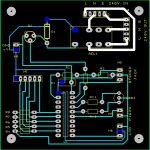
I'd like to move on to the next stage of making the PCB so any comments on the schematics and PCB will be very much appreciated.

Thanks


20X2_With_Relay-2.jpg20_X_2_With_Relay_V1_PCB.jpg
 

SAborn

Senior Member
In fear of upsetting you i hesitate to comment, but what the heck.

Why do you have such weedy little tracks between components when you have room to use chunker tracks like you used for the relay.

I look at it this way, you start with a full copper clad board and then remove 95% of the copper, why? when you can leave it there.

This reduces problems when exposing and etching boards, extends the copper life with exposure to the elements, allows for easier changes if needed, and extends the life of your etchant, with increased etching times.
Not to mension lower track resistance or less voltage drops over track lengths and strength to component mountings.

I once too use to do weedy little tracks to i realized it was to a disadvantage, and suffered from some of the above problems.
 

EricD

Member
In fear of upsetting you i hesitate to comment, but what the heck.
I have over 20 posts now so it's ok to upset me. LOL (just kidding)

Why do you have such weedy little tracks between components when you have room to use chunker tracks like you used for the relay.

I look at it this way, you start with a full copper clad board and then remove 95% of the copper, why? when you can leave it there.

This reduces problems when exposing and etching boards, extends the copper life with exposure to the elements, allows for easier changes if needed, and extends the life of your etchant, with increased etching times.
Not to mension lower track resistance or less voltage drops over track lengths and strength to component mountings.

I once too use to do weedy little tracks to i realized it was to a disadvantage, and suffered from some of the above problems.
The main reasons for using weedy little tracks are simply because I don't know any better. Mind you I have had the problems that you mention above.

All the PCB programms that I tried out are all set up for weedy little tracks. Also, all the Videos I watched on Youtube and elsewhere on the Internet all seem to use small tracks for low voltages and chunkier tracks for higher voltages. From this I gathered that it is the normal thing to do so I did the same.

Originally the DesignSpark "default" track size is set to 0.3810, I changed them to 0.5 after I placed the components in their places and connected them together.

To extend the life of the etchant, I usually do copper pouring. In other programms I had success with that but in DesignSpark the gap bettwen the copper and tracks is very fine and I have not been able to find a way to increase this gap. The first PCB I made using DesignSpark was so fine that it was almost impossible to solder without shorting the parts to the copper or to each other. This time I left the copper pour out and spaced the parts further apart so that I don't have the same problem.

What size tracks would you suggest I use?

Thans for your reply.
 
Last edited:

MartinM57

Moderator
I would go with something like the DesignSpark equivalent of 30mil (0.030") for general purpose, low voltage, low density (i.e. not many of them) tracks

If Design Spark doesn't allow you to specify the pour-to-track clearance, then it's not very good :D
 

SAborn

Senior Member
One way of looking at track size and what size to use, is look at the pad sizes and as you can etch the pads ok with clearance then a track size close to the pad size should allow enough clearance, personally i try to stay above 1mm unless i need to squeeze through some where. (no idea what 1mm is in inches but 0,030" sounds about correct)
Fat tracks can look a little goofy on the screen but once etched they look neat and if not better than little weedy tracks on this large board area.

Never used design spark but the default clearance settings is often located in board properties.

A copper pour is a good thing to add, and a clearance of 0.6mm to 0.8mm is often what i use, even though i can go finer there is no point in making life harder with assembly and increased risk of bridges in the etching.
 

Dicky Mint

Senior Member
Why not try Sprint Layout?

Its not free (~£33) but it gives a lot more control over pad, track size and clearance of copper pour
and in my opinion, produces an more elegant solution than others I've tried.

Just a thought
 

EricD

Member
@MartinM57, there may be a way in DesignSpark to increase the pour-to-track clearance, I just have not been able to find it.

0.030" is 0.762mm, I used 0.5mm. I will increase the tracks to 0.762, or higher where possible.

Thank you both for your replies, really appreciate it.

I can now finish my project and start on the next one, a small CNC. I want to start with a small one to get the experience then move on to a bigger one which I can use in my woodworking projects, wish me luck.

Thanks again.
 

nick12ab

Senior Member
@MartinM57, there may be a way in DesignSpark to increase the pour-to-track clearance, I just have not been able to find it.
Right-click the area with copper poured in it, click Properties and find the width property at the top of the dialog that appears and reduce the number.
 

SAborn

Senior Member
I can now finish my project and start on the next one, a small CNC. I want to start with a small one to get the experience then move on to a bigger one which I can use in my woodworking projects, wish me luck.
I have made several of these CNC machines and they are well worth the time and effort, best thing since sliced bread (well they will even slice bread to if you want).

I can offer some help and advice if you would like, on where to get stepper motors and what driver boards work well at cheap prices etc, if you can put up with my "cultural nuances" as i think it was put? (i had to google that to find out what it was)

Feel free to Message me if you would like some advice.
 

inglewoodpete

Senior Member
Going back to your board design, I would do 2 things with the layout.

1. Most important! Reverse the Line and Neutral connections. That long trace at 230v AC, especially near the mounting hole, is potentially lethal. Make the 'Line' trace the short one.

2. (Opposite corner) Move the other connector away from the mounting hole to give you more space for mounting the board. I use 3mm screws and spacers - they need a little space.
 

EricD

Member
Going back to your board design, I would do 2 things with the layout.

1. Most important! Reverse the Line and Neutral connections. That long trace at 230v AC, especially near the mounting hole, is potentially lethal. Make the 'Line' trace the short one.

2. (Opposite corner) Move the other connector away from the mounting hole to give you more space for mounting the board. I use 3mm screws and spacers - they need a little space.

Thanks for pointing that out inglewoodpete, I've done both.
 

Paix

Senior Member
Thanks for the DesignSpark info Eric, I have made a note of it and will be that little bit more enlightened when I next try to get to grips with DesignSpark. :)

Seems like you have reached a happy final design too.

Regards,
Ian
 

EricD

Member
Thanks for the DesignSpark info Eric, I have made a note of it and will be that little bit more enlightened when I next try to get to grips with DesignSpark. :)
You are welcome, not that I can help much here but I'll do what I can.

Seems like you have reached a happy final design too.

Regards,
Ian
Yes, I am very happy with that and will be happier when it gets warmer so that I can get in the garage and build it into the UV box. It's snowing again and it's about freezing, the box can wait. LOL

Thanks again everyone for all your help.
 

EricD

Member
Why not try Sprint Layout?

Its not free (~£33) but it gives a lot more control over pad, track size and clearance of copper pour
and in my opinion, produces an more elegant solution than others I've tried.

Just a thought
Sorry Dicky, somehow I missed your post. I only do electronics as a hobby a few times a year at the most so can't really justyfy spending that sort of money on a program. The reason I use DesignSpark is because you can download MB schematics and pcb layout for picaxe chips, relays circuits plus a few other things, guite helpfull for a beginner like myself. Plus, all the chips etc are included in the components library. It's actually not a bad program, better now that I know how to change the track-to-copper pour.
 
Top