PC board fabs

julianE

Senior Member
Gents,

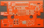
I've been shopping for pc board makers and it's gotten expensive since I last ordered boards back in 2015. I used a couple places back then, one was dirtypcbs.com, they did a nice job but the shipping is more expensive than the boards. Any suggestions, are there any inexpensive US based pcb makers?
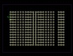
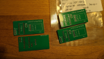
I don't need anything complicated. double sided simple boards. I have been using this 5x7 cm protoboard that's a clone of an old radio shack board for a long time, would be even better if it were double sided.
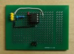
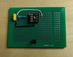
While I'm asking questions, what is the most basic, easiest to learn free pc cad, i have the eagle cad. it's very good but way more than i need. I'd like to make that same version of radio shack protoboard but in different sizes and maybe the picaxe download circuit.

thanks in advance and a happy new year to all.
 

papaof2

Senior Member
DipTrace might be the simplest I've used. There was a free version for PICAXE users that covered a double-sided board with 300 or 500 connection points (device/part pins and external connections). Maybe search the forums for a link?
 

Solar Mike

New Member
Diptrace is very easy and intuitive to learn, the lite version is free for non-profit use, send them a note to get the download link.
Link: DipTrace

JLCPCB are where I get my PCBs made, very inexpensive, the cheapest shipping option, airmail courier takes about 10 days delivery to NZ.
Export your diptrace gerber files to a folder, then zip it up, drop the zipped file on the JLCPBC load page to preview and get costs.

Cheers
Mike
 

oracacle

Senior Member
A second for JLCPCB. I normally get inside of 2 weeks to the UK. The only mistakes that I've gotten from then are the ones I made in the design.
 

Jeff Haas

Senior Member
The quality of the JLCPCB boards is great, especially for the low price. The edges are even smoothed down!

Here's a snap of some CH340 adapter boards I made, following the design elsewhere in the forum:

25599
 

julianE

Senior Member
Here's a snap of some CH340 adapter boards I made, following the design elsewhere in the forum:
beautiful boards.

I downloaded Diptrace and will set up an account with JLCPCB.
Once I design my first board I hope someone can spare the time to look over the design, it will be something very simple, a protoboard.
Grateful, as always, for all the help.
 

Jeff Haas

Senior Member
You will get better quality than those knock-off Radio Shack boards. Consider any personalizations you might want, it's great to get a board the way you designed it.
 

lbenson

Senior Member
In the U.S., I occasionally order boards from oshpark.com--usually only very small boards--they're $5 per square inch for 3 boards. Delivery is comparable to JLCPCB. For bigger boards, JLCPCB is less expensive--5 boards 100mm x 100mm or smaller for about $6.38US with Paypal and slow boat shipping (about 3 weeks).

By the way, utility SIP (single in-line pin) PICAXE boards ready for ordering (gerbers, with EagleCad sch and pcb files available for your customization) can be found here: 08SIP, 14SIP, 20SIP PCBs. Very breadboard friendly.

Another version of the Goeytex / Erco programmer board is here.
 
Last edited:

julianE

Senior Member
By the way, utility SIP (single in-line pin) PICAXE boards ready for ordering (gerbers, with EagleCad sch and pcb files available for your customization) can be found here: 08SIP, 14SIP, 20SIP PCBs. Very breadboard friendly.
For our younger forum members, I can't overemphasize, "Do Not Get Old", I did a search through my emails and I already have an account with JLCPCB and OSH Park. Had them send me my log in info and I'm good to go. I ordered Lbenson's 08SIP boards from OSH Park back in 2014 I used one a few weeks ago. I also ordered a larger board posted by a kind member, it was very expensive with OSH Park, I did get a bunch and still have some in stock. Getting scary how much I forget as I get older, fortunately it does come back with a slight reminder.

Watched a video on using diptrace, will give a try later in the day.

as always, molto grazie.
 

lbenson

Senior Member
I ordered Lbenson's 08SIP boards from OSHPark back in 2014 I used one a few weeks ago.
Glad to hear they've actually been ordered and used.

"Do Not Get Old"
At 76, I continue to find the alternative unappealing. And "You're only as old as you think you are" is, ummm, aspirational. But it helps to try to keep the little grey cells operational.
 

bogbean

Well-known member
beautiful boards.

I downloaded Diptrace and will set up an account with JLCPCB.
Once I design my first board I hope someone can spare the time to look over the design, it will be something very simple, a protoboard.
Grateful, as always, for all the help.
I am also impressed with JLCPCB boards. I started with Eagle for laying out PCBs but then switched to Kicad. I found the learning curve ok and the support (forums and YouTube) to be good. Whichever package you use I think it’s just good to get started and build up experience designing boards. And yes do post your drafted design for people to look over.
 

Tvmender

Active member
JLC are great, ordered many times from them and they haven't missed a beat. Very competitive pricing and reasonable delivery times. I use Eagle and PCB Wizard.
 
Last edited:

steliosm

Senior Member
I also use JLCPCB for my PCBs. I design the circuits using Fritzing and send the exported Gerber files. Never had an issue on the PCBs and most of them are used for SMD chips.
 

julianE

Senior Member
Here's a snap of some CH340 adapter boards I made, following the design elsewhere in the forum:
The 3 pin header labeled "to PICAXE" the pins don't look to be inline, I have seen that on other designs. I like to use 3 pin cables and wonder if it would cause issues.
 

julianE

Senior Member
Thanks for all the replies. I tried designing my first board in DipTrace and it's slow going. Some of the difficulty is due to overabundance of different parts, I can see that getting easier once a collection of often used parts is made. Much respect for the folks that have figured all this out, I'm certainly not the smartest in this room :)
 

Jeff Haas

Senior Member
What you see on those boards for the Picaxe and CH340 headers is an idea from Sparkfun. A friend of mine there figured out that if you make a set of pins slightly zig-zag, the header doesn't fall out when you solder it in. So now whenever I create a header I use their tip.

Full details in this blog post:
 

bogbean

Well-known member
Well done persevering to get your protoboard drafted. Here are my comments but be aware that I am a KiCad user and not familiar with DipTrace. I have used JLCPCB though.

The screengrab seems to show a copper layer with pads and traces but I see no holes inside the pads. Have you used plated through holes? If you generate the gerber files for JLCPCB to manufacture with you should be able to check that the copper pads line up with the holes that need to be drilled. I recommend doing that. This is my only comment that could affect receiving a board that is functionally usable, everything below is 'a nice to have' or perhaps something to consider in future revisions. Sorry to throw a lot of points at you, I actually encourage you to ignore them and just order what you have already! It's good to just get over the hurdle of getting your first boards ordered and received.

I recommend putting non-plated through holes in the corners of the board, they often come in handy (I generally use holes sized for M3 PCB supports).

I assumed you intentionally have the gap in pads over on the right hand side and the asymmetric hole arrangement either side of the power rails.

It may be sensible to user wider copper traces for the power rails since they will carry more current. That would also help make them visibly stand out as power rails.

I recommend googling 'JLCPCB DipTrace' for JLCPCB advice and other forum advice on generating gerber files that JLCPCB will accept and that comply with their manufacturing capabilities.

JLCPCB will add an order-tracking number in the silkscreen layer. If you have a preference for the location of that number you may add the text 'JLCJLCJLCJLC' on the silkscreen layer in the location of your choosing. Otherwise it's up to them where they put it, it may be somewhere annoying.

JLCPCB will allow you to choose the colour of your soldermask. I'm often tempted to get boards in black because I like how they look but it's much easier to see the actual copper traces with a non-black soldermask. Being able to clearly see your copper traces could be handy for a protoboard.

When you upload your zipper gerber files to JLCPCB they have a 3D viewer you can use as a final check of your design. DipTrace may have a 3D viewer too.

I recommend adding a few things in a silkscreen layer:
  • row / column hole numbering labels
  • Perhaps + / - labels to your power rails.
  • A revision number for this design. In case you modify your design in the future it's handy for the board to be printed with the revision number on it.
I've just realised from your original post that you've done pcb design before so forgive me if I'm teaching you to suck eggs here...


pins slightly zig-zag, the header doesn't fall out when you solder it in
+1 for this being a clever idea
 
Last edited:

julianE

Senior Member
I actually encourage you to ignore them and just order what you have already! It's good to just get over the hurdle of getting your first boards ordered and received.
I am in production, got this message today,

Production Progress

Estimated finish time: 2023-01-06 20:56:02

Thank you for taking the time to make excellent suggestions. Last night I uploaded my gerber files to different fab places, prices were all over the place, some as high as $30 for 3 boards. Last one to try was JLCPCB, a little over $12 shipped for 10 boards, I'm guessing that's a promotional price, if it's not I'll be making a lot of boards. At that price I could afford to make mistakes, I placed the order.

The holes are plated through. I did want to make the traces thicker all around and pads a little bigger, my concern was it would get rejected so I went with the default setting of DipTrace. The asymmetry is intentional and I left the row empty because of the limit of holes imposed by the free version of diptrace and to give the board a bit of a distinguished feature. I wanted the board as simple as possible to increase chances of success and to make it as universal as I can. I also dabble with raw microchip pics so the download cable isn't always the same. As far as labeling power rails that I agree should be thicker I left them unlabeled because non microcontroller chips have the positive on right side of the chip and i orient the power supply to match the chip used.
I forgot to have the corner mounting holes drilled.

I'm not married to DipTrace and my guess is once you get proficient at one software it's not much of a leap to switch. I think the free version of KiCad allows for larger boards.

Thanks for all the input, I could have never done it on my own. I will update the forum once the boards arrive. In the meanwhile I'll work on adding all the suggestions for my next revision.

Happy New Year.
 

MartinM57

Moderator
It may be of interest and it's not a great photo, but this is my latest suitably licenced Diptrace/JLCPCB double sided board...about 270 pins IIRC, 160mm x 100mm
25606

"Cheap" parts (Resistors, capacitors and diodes) have been assembled by JLCPCB and they've done an excellent job. You have to jump through hoops and it's a bit time consuming to specify the assembly details, including getting the part numbers to use, but if you're making a lot (or you just want to do because you can) it's well worth it.

Some "cheap" parts are not assembled in this prototype board - if you have slightly odd, say, resistor values (eg 680R for some of mine) then although they have them, they charge a few dollars per component (not per board) to, I imagine, get a person files to load the reel into the assembly machine. The reels for the common components e.g. 100n capacitors are probably always loaded.

As this board is pretty sparse, I use 1206 layouts but get them to assemble 0805 components as they are fractionally cheaper, and if I'm hand soldering I also have 0805 components that are very easy to hand solder to 1206 pads.

JLCPCB will assemble down to 0402 components. or even 0201 if you use their Standard (not Economic) fab option.

I would never get JLCPCB to assemble anything more than SMT resistors, capacitors and diodes - they offer many more higher level components but their sourcing of them is unclear.

The top left and bottom right holes have been added by JLCPCB to mount the boards in the assembly machine. Other smaller boards I've had assembled have the holes only 1mm or so from the corners.

There's a couple of components on the other side, so there's a Bottom Silk layer - JLCPCB have put the order number on that layer, without me asking.

JLCPCB don't offer two-sided assembly,

The red PCB colour (FOC) and assembly only added 1 day or so the the elapsed time their side, but maybe they weren't too busy over Christmas.

(not a PICAXE project unfortunately, but I did prototype bits of it with a PICAXE and use PICAXE-based pulse/serial data generators for development and testing)

No doubt the PCB Layout Police will chip in, but any potential improvements would be considered ;)
 

lbenson

Senior Member
Last one to try was JLCPCB, a little over $12 shipped for 10 boards, I'm guessing that's a promotional price, if it's not I'll be making a lot of boards.
Their "promotional price" has been in effect for a good many years. I tend to get 5 boards for $6.38US with the slow shipping. Can't be beat.
 

oracacle

Senior Member
Those is my recent project that needed boards made. Made some jigs to hills the solar paste mask in the right place. Really can't complain about the quality
 

julianE

Senior Member
I tend to get 5 boards for $6.38US with the slow shipping.
I will be ordering boards weekly, there are so many projects that are held back because of difficulty of point to point wiring, audio projects in particular. Digital projects I don't mind doing on protoboards.

If the shipping costs are lower I'll do multiple projects at the time.
 

bogbean

Well-known member
I think the free version of KiCad allows for larger boards.
KiCad is open source so is free and has no limits on board size that I've found yet. I think the JLCPCB price jumps up a bit if your board exceeds 100mm in either dimension, but is still very reasonable. Interested to hear how your boards turn out.
 

lbenson

Senior Member
If the shipping costs are lower I'll do multiple projects at the time.
The $2 price for the first PCB goes to $5 for the second, so you save very little by bundling designs. If I had one project done and figured it would take a day or two to finish a second, I'd probably order them separately. If I finished a design and had an older one I wanted more copies of, I'd bundle them.

In the last 4 years and 2 months, I've placed 63 orders with JLCPCB (a few of those were designs by others).
 

julianE

Senior Member
The $2 price for the first PCB goes to $5 for the second, so you save very little by bundling designs
Good to know, wow 63 orders, you must buy solder in bulk :)

I need to find how to print the PC boards actual size on a laser printer so I can get a feel for the true size of pads and spacing.

KiCad is open source so is free and has no limits on board size t
I'll be downloading KiCad today. Thanks for the info.
 

papaof2

Senior Member
Printing to size -
Some image manipulation programs have the option of "Print actual size" or similar wording so you can do that. Even my ancient copy of PolyView (copyright dates i1995-2011) has that option.
See what options are under "Print".
 

julianE

Senior Member
That JLCPCB is very impressive, the boards have made it to USA. It will be a week since I sent it in. Very good updates all along. Hopefully the boards will be in in my mailbox soon.
 

Jeff Haas

Senior Member
It usually takes a few days for the US shipping company to hand it off to your local post office. Then it arrives quickly.
 

julianE

Senior Member
Thanks to Erco post about Robot Mesh store going out business sale I have a good stockpile of 18M2 chips and my next protoboard will be geared towards 18M2 chips, I'd like it to be a smidge larger so I'll be using eaglecad or KiCad. my current board will work just fine with the 18M2 other than for less space.
 

erco

Senior Member
Awesome! Ha, just this morning I saw that cap-under-the-socket trick at another website. Clever! I put both .01 uF disk and 10 uF electrolytic caps on my boards. Probably overkill but that's how I learned. Jeff Haas & I both have a bunch of 18M2s as well, he's a prolific PCB maker. Only a matter of time before he makes a board for that. IIRC he's working on a 20M2 board now.
 

julianE

Senior Member
I sent in my second board, it was a struggle to get it under 100mm. Turns out as soon as it's larger than 100mm there is a $4 "engineering fee" and the board prices go up as well. Being on the cheap side of thrifty I spent an hour rearranging components to shrink the board to 99mm.
5 boards for around $10 delivered.

I'm not sure how others do it but I find drawing a schematic in diptrace a waste of time. The way the program arranges the components on the board is a jumble that takes too long to untangle. I find it easier to have a printout of the schematic and arrange the components manually in the PCBLayout window. I also waste a lot of time looking for components, I needed a JFET with the middle pin being the gate, took a while to find one.
I'm guessing it will all get easier with use. I'll start working on the next board, it's nice having a sample board for figuring out spacing of components.
 

Tvmender

Active member
I use the free version of Eagle PCB which limits the size to 100 x 80mm. These seem to fall within the cheap bracket for manufacture. Where I needed larger boards I "stack" them using hex spacers and join with ribbon cable. I ordered about 15 boards which came to less than £30.00. The delivery was more than the manufacture!

To save more space I have a couple of designs where the PICAXE is soldered onto the board in its RKP20c breakout board with header pins. I can then use the space beneath the PICAXE and all the programming components, socket etc. are on the RKP20c saving more room.
 
Top