Nearly, but not quite.
ALL MOSFETs (P and N) have a significant capacitance. Check out the Data Sheet figures usually under the heading "Dynamic Characteristics". You will see a bunch of pFs.
For
fast stuff you
need a driver to suck that charge out and shove some omph back into the gate regardless of N or P channel.
You highlighted a N channel driver for High/Low. Well, it's doing the sucking and shoving but at the voltages necessary to make an N channel work as a high-side driver - it relates to gate/source voltage.
A P channel driver does a similar thing but it will take the gate down to nearly Gnd/0V and shove it back up to Vss with great gusto. Remember, you need to get a pile of coulombs out and back in at f.High speed - ideally < 250nS. Do the maths for instantaneous current.
Obviously the greater the R/Z component in your driving the slower that Gate charge is sucked/shoved, as you'll know from any R/C circuit with your exponential curves.
For an easy life switching a 'Logic' level N channel as a low sided switch is a piece of cake, but do rmember, you STILL have capacitance. A PIC o/p is incapable of doing a fast job. It can do it , of course, but not at a 'speed' good enough for fast high-power PWM.
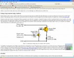
That little NPN/P-Chan combo: the NPN will suck the charge out of the gate reasonably well, but it relies on the resistor to shove it back when the NPN switches OFF. So, if you looked at the MOSFET output you would see a sharpish leading edge of a square wave and a soft trailing edge. You could improve the performance by replacing the Gate-NPN res with a low one say 47R and replace the Gate/Vss res with say 470R, but this increases the current just to make it work.
For the lower-end Power MOSFETs and light load this is OK. But those non-sharp waves mean that the MOSFET is spending a significant amount of time as a resistor. For PWM and a heavy load this is NOT good.
And as you turn up the frequency or shorten the duty-cycle those soft edges become even more significant as a percentage compared with full on/full off. In fact it could end up looking like sawtooth wave - bad!
When the MOSFET acts as a resistor, there is a painful consequence. Good old IsquaredR.
A proper driver essentially replaces the piddly signal-level NPN with something more manly and replaces the Gate/Vss resistor with something that is a low resistance/impedance path to Vss - but operates exactly out of phase with the NPN side, ideally to get a strong, sharp IN/OUT/IN/OUT to the Gate with no overlap.
If you look at some of the drivers linked earlier using discretes you should get the picture as to the principle of operation. Drivers are basically a well designed, complimentary pair which are well matched and can handle a high current from a logic input.
Many driving circuits can also suffer from 'shoot through'. No I didn't make that up. It means where both of the arms of the complimentary pair are on and the current shoots through wastefully. An ideal driver has none.
There are many poblems getting a home-brewec driver circuit to work well, and unless you want something special and you have the experience/equipment to do it, just go and buy a driver chip. For fast/efficient/cool PWM you will need it, for N or P channel.
However, if it a learning thing then DO experiment with discretes, it will be very useful experience.. if you have the time you will gain a lot of knowledge. Mind you, if you don't learn then you'll be back here wondering why it doesn't work
")
If you truly want to get to grips with all this then go to some Manufacturers's sites and get their Application Notes on driving FETs. They can explain it far better than my efforts. And once you have absorbed, learned and tried then you can tell others. Just remember: components aren't 'perfect'.