PhilHornby
Senior Member
I've been experimenting with the code in this thread to modulate a (PWM-derived) 125KHz carrier using the Data Signal Modulator. I've chosen to use the 'MDMin' pin to modulate the data - and this behaves differently on the 14M2 and the 08M2 (aka PIC16(L)F1825 and PIC12(L)F1840) - despite the datasheets being identical.
In a nutshell, the MDMin pin (C.0 on 14M2 and C.1 on 08M2) is the subject of 'output' commands such as
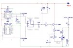
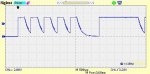
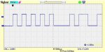
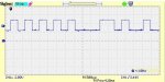
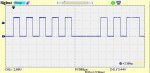
All was fine, until I tried to take this signal to an external circuit, in order to generate 10µS pulse to fire a Triac. It seems that C.0 pin on the 14M2 pin is in full 'output' mode, whereas C.1 on the 08M2 behaves much more like an 'input' with the pullup activated. I want to generate the pulse on the falling edge of the signal and on the 08M2 there isn't a falling edge, unless I add a resistor to GND!
Is this expected? Is there something I can configure to change it to a 'proper' output? (I believe I've tried every thing specifically related to the DSM that might apply).
I can always add a some more hardware - but it would be nice if I didn't need to.
This is my code for initialising the DSM. Aside from the comments, it is identical on the two PIC(axe)s.
14M2 Base PIC datasheet
08M2 Base PIC datasheet
In a nutshell, the MDMin pin (C.0 on 14M2 and C.1 on 08M2) is the subject of 'output' commands such as
HIGH and PULSOUT, but the DSM sees the signal as though it is an input.All was fine, until I tried to take this signal to an external circuit, in order to generate 10µS pulse to fire a Triac. It seems that C.0 pin on the 14M2 pin is in full 'output' mode, whereas C.1 on the 08M2 behaves much more like an 'input' with the pullup activated. I want to generate the pulse on the falling edge of the signal and on the 08M2 there isn't a falling edge, unless I add a resistor to GND!
Is this expected? Is there something I can configure to change it to a 'proper' output? (I believe I've tried every thing specifically related to the DSM that might apply).
I can always add a some more hardware - but it would be nice if I didn't need to.
This is my code for initialising the DSM. Aside from the comments, it is identical on the two PIC(axe)s.
Rich (BB code):
symbol MDCON   = %11111100          ;Control
Symbol MDSRC   = %11111101          ;DSM Source select
symbol MDCARL  = %11111110          ;DSM CarrierLo signal select
symbol MDCARH  = %11111111          ;DSM CarrierHI signal select

;Data Signal Modulator
;Register 23-1 MDCON: Modulation Control Register

symbol MDEN=bit7  ;  1-------       ;Modulator module is enabled and mixing input signals
;MDOE             =  -1------       ;Modulator Pin output enabled (C.0 aka Serout on 08M2)
;MDSLR            =  --0-----       ;MDOUT pin slew rate limiting disabled
;MDOPOL           =  ---0----       ;Modulator output signal NOT inverted
;MDOUT            =  ----R---       ;Current value (readonly)
;unimplemented    =  -----XX-       ;Unimplemented
;MDBIT            =  -------0       ;Select LOW Carrier source (only when MDBIT selected in MDSRC)
symbol valMDCON   = %11000000       ;composite of above

;Data Signal Modulator
;Register 23-2 MDSRC: Modulation Source Control Register

;MDMSODIS         =  0-------       ;Output signal driving peripheral selected by MDMS<3:0> is enabled
;unimplemented    =  -XXX----       ;Reads as 0
;MDMS             =  ----0001       ;0001 = MDMIN port Pin (C.1 on 08M2)
symbol valMDSRC   = %0000001        ;composite of above

;Data Signal Modulator
;Register 23-3 MDCARH: Modulation High Carrier Control Register

;MDCHODIS         =  0-------       ;Output signal driving the peripheral o/p pin is enabled
;MDCHPOL          =  -0------       ;Selected High Carrier Signal is NOT inverted
;MDCHSYNC         =  --0-----       ;Modulator o/p is NOT synchronised to the high time carrier
;Unimplemented    =  ---X----       ;Unimplemented
;MDCH             =  ----0100       ;0100 = CCP1 output (PWM mode only). (Normally C.2 on 08M2)
symbol valMDCARH  = %00000100

;Data Signal Modulator
;Register 23-4 MDCARL: Modulation Low Carrier Control Register

;MDCLODIS         =  0-------       ;Output signal driving the peripheral o/p pin is ENABLED
;MDCLPOL          =  -0------       ;Selected Low carrier signal is NOT inverted
;MDCLSYNC         =  --0-----       ;Modulator o/p is NOT synchronised to the low time carrier
;unimplemented    =  ---X----       ;Unimplemented
;MDCL             =  ----0000       ;VSS
symbol valMDCARL  = %00000000       ;composite of above

      PokeSfr MDSRC,valMDSRC                    ;set Modulation Source Control Register
      PokeSfr MDCARL,valMDCARL                  ;set Modulation Low Carrier Control Register
      PokeSfr MDCARH,valMDCARH                  ;set Modulation High Carrier Control Register
PokeSfr MDCON,valMDCON ;set Modulation Control Register08M2 Base PIC datasheet