Will a 08 Starter kit be able to program a 14 or higher
- Thread starter Protolisk
- Start date
In theory yes, you can just put the top 8 pins of the 14/20 chip into the 8 pin socket, but you may end up with bent pins! A better way would be to use a 20 pin project board to program 14 and 8 pins, as the socket will fit all 3 in that case.
However we would not recommend that either, the PICAXE system is based upon building the download circuit into every project board...
For 14 and 20 projects boards see parts AXE117 and AXE118.
You could not program 18, 28 or 40pin in this way as they have different layouts.
However we would not recommend that either, the PICAXE system is based upon building the download circuit into every project board...
For 14 and 20 projects boards see parts AXE117 and AXE118.
You could not program 18, 28 or 40pin in this way as they have different layouts.
Last edited:
hippy
Ex-Staff (retired)
A piece of strip-board / vero-board or PCB with the range of PICAXE-size sockets on can quite easily be built with a single download interface, single reset button and even a 7805 regulator. This is very handy for testing and programming for circuits which do not have a download socket.
Use high quality turned-pin sockets for durability. Serial In, Serial Out and Reset goes to the respective pins of each socket so only one PICAXE can be used in the board at any one time. For 28/A/X and 40X give each their own 4MHz resonator; these are optional if only using the 28X1 and 40X1.
I'd definitely add a power LED plus LED's to indicate Serial In and Serial Out activity.
An alternative is to build a small board with just the download interface and a single DIL 'socket' built from two female Molex sockets and then build plug-in adapters for each PICAXE size you need.
Both methods can also be used for ICSP programming of PICmicro's out of circuit. It should be possible to have a single board which can do both; PICAXE download and Microchip ICSP. Care needs to be taken with circuit design to handle PICAXE's which may set the ICSP pins to outputs at power up.
No.
See Technical's post #2
The issue is the pin layout.
The serin/out and power +, 0 need to be in the same relationship to each other.
Manual1 has the pin layouts for the range of PICAXE chips.
You can see by comparing those diagrams that legs 1 & 2 and the pair opposite are always the same for 08, 08M, 14 and 20 so these could all fit in the same socket by ensuring Chip leg 1 is always in the socket leg 1 and avoiding pin damage (use a socket of the right size on top of the socket in the board).
For the others - , these relationships are different from each other, and from the 08/08M/14/20 group. The 18, 28 & 40 also need the reset circuit (or at least the pullup) adding.
So that is a minimum of four different incompatible layouts.
To do what you want you need a 'universal programmer'. Build it from strip board as suggested by Hippy, a breadboard, make a special, or incorporate the download circuit on your project. If you check the minimum operating circuits for each PICAXE you will find that virtually all the download components (except the connector) are required anyhow.
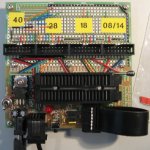
An example of a Universal programmer handling 8 thru 40 pin PICAXEs is shown below. The chip to program is selected by using the plug at bottom right and inserting it into the appropriate socket below the labels. This ensures all the necessary programming circuits are properly connected and includes power supply and reset.
This was built on a KPIC prototyping board and uses a ZIF (zero Insertion Force) socket to ensure no leg damage.
See Technical's post #2
The issue is the pin layout.
The serin/out and power +, 0 need to be in the same relationship to each other.
Manual1 has the pin layouts for the range of PICAXE chips.
You can see by comparing those diagrams that legs 1 & 2 and the pair opposite are always the same for 08, 08M, 14 and 20 so these could all fit in the same socket by ensuring Chip leg 1 is always in the socket leg 1 and avoiding pin damage (use a socket of the right size on top of the socket in the board).
For the others - , these relationships are different from each other, and from the 08/08M/14/20 group. The 18, 28 & 40 also need the reset circuit (or at least the pullup) adding.
So that is a minimum of four different incompatible layouts.
To do what you want you need a 'universal programmer'. Build it from strip board as suggested by Hippy, a breadboard, make a special, or incorporate the download circuit on your project. If you check the minimum operating circuits for each PICAXE you will find that virtually all the download components (except the connector) are required anyhow.
An example of a Universal programmer handling 8 thru 40 pin PICAXEs is shown below. The chip to program is selected by using the plug at bottom right and inserting it into the appropriate socket below the labels. This ensures all the necessary programming circuits are properly connected and includes power supply and reset.
This was built on a KPIC prototyping board and uses a ZIF (zero Insertion Force) socket to ensure no leg damage.
Attachments
-
 763.1 KB Views: 28
Last edited: