Why are there two GND (0V) pins on 28X2? Do I need both?

popchops

Well-known member
Hi there!

I am designing a PCB for a fully tested circuit. I found an EDA Symbol for the PICAXE chip, or at least I thought I could use the Microchip PIC18F25K22-xSP Symbol (below). However - after completing all other parts of the circuit I just noticed that pin 19 is missing! Does anybody know why? Is Pin 19 tied to Pin 8 internally?

25490
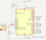
My (fully functioning) prototype is implemented as per Picaxe Manual1 page 35, including 0V connection to pins 8 and 19.
25491
Why would the microchip Symbol have deleted pin 19??

Thanks!!!

Popchops.
 

AllyCat

Senior Member
Hi,

The Microchip Data Sheet shows both pins as "Vss" so they are probably connected internally, but not necessarily by a low-resistance path (e.g. two separate connections to the Silicon Substrate). Therefore, IMHO both pins should be connected externally by a low impedance path, and I believe there have been Forum posts from members who have encountered "issues" when this was not done.

That pin 19 is not shown at all, suggests that the EDA Symbol is "faulty", since the package requires at least a through-hole or pad for every pin.

Cheers, Alan.
 

popchops

Well-known member
Hi,

The Microchip Data Sheet shows both pins as "Vss" so they are probably connected internally, but not necessarily by a low-resistance path (e.g. two separate connections to the Silicon Substrate). Therefore, IMHO both pins should be connected externally by a low impedance path, and I believe there have been Forum posts from members who have encountered "issues" when this was not done.

That pin 19 is not shown at all, suggests that the EDA Symbol is "faulty", since the package requires at least a through-hole or pad for every pin.

Cheers, Alan.
Thanks Alan.

The associated footprint is correct- it's a 28 pad footprint. But the symbol is missing one. I'll edit the symbol to add the missing pin.

Really I just wanted to know what is the common practice with pin 8 and pin 19, and you answered that.

Thanks, Pops.
 

inglewoodpete

Senior Member
Both pins need to be grounded. While they are both connected together through the silicon of the chip, the current carrying capability and the internal resistance of the silicon path alter the performance of the chip if both pins are not connected together externally. In many circumstances, the ground reference voltage level can rise beyond design specification levels if not held down with a low impedance/resistance path. Also, when many I/O pins are carrying their maximum rated current, heating of the substrate can occur, affecting the performance of the chip.

You may notice that the 40X2, a chip with very similar silicon but more pins, has duplicated Vdd and Vss pins for the same reasons. In the case of the 40X2, decoupling capacitors must be connected across both pairs of pins.
 
Top