Hi,
The Data Signal Modulator (DSM) is an optional Logic module contained in all M2 PICaxes. The base PIC data sheets explain how it can be used for complex modulation schemes such as FSK (Frequency Shift Keying) or Amplitude modulation (AM or On-Off Keying, etc.), but the aim here is to show how it can be used to replace simple external hardware such as a latch or inverter (for example to invert the HSERIN signal).
The following diagram, taken from the base Microchip (18M2) data sheet, has been annotated with the Logic functions, Special Function Register flags, External Leg numbers (for 8, 14, 18 and 20 pin chips) and sample internal logic states. This diagram is similar to that created in response to a question in a recent thread (post #19), but I have changed the SFR flag values slightly, to simplify the setup for all three possible input pins.
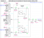
To implement a simple inverter we need a single "active" path (between the chosen input and output pins), with the remainder of the DSM "passive" (i.e. stable). To minimise the number of flags which need to be set, the "High" path was chosen to be passive (i.e. blocked) and the "Low" path (including the modulation block for its associated input pin) being active.
For the active signal to pass though the OR gate at the output of the DSM module, its upper (unchanging) input must be Low (logic 0). Then, working backwards towards the upper input multiplexer, we see that all the relevant flags and input selector can be set to 0. Conversely, the lower AND gate needs to pass a signal through from either the Modulation Input or the "Low" input (depending on the desired input pin), so we set both of its inputs initially to a 1 (high) state. Hence the choice of the active modulation path via the NOT gate, and setting the flag into the XOR, to invert the fixed Low (Vss) input. Finally, we must set the SFR flags to select the required input pin, and the hardware Enables (DSM, OE, etc.).
The above code should configure the DSM to act as an inverter for the selected input of any M2, but has not been comprehensively tested. However, the 08M2 is rather limited because the DSM output employs the same pin as the Serial (Programming) output, and also it is rather greedy of pins. But it is possible to test/demonstrate the DSM using only the normal programming cable by connecting the DSM in series with the HSEROUT signal, which can be linked internally to the Modulation multiplexer (input 10 decimal). However, this is not a very useful facility because the HSEROUT hardware already includes an inversion capability; it is the HSERIN inversion (to the normal PICaxe idle-low) which is not programmable in M2s.
Furthermore, it is possible to implement HSERIN and HSEROUT of both polarities (software-selectable) in an 08M2 by using the Alternate Pin Function (APFCON , 4) SFR to move HSEROUT onto Leg 3, thus releasing Leg 7 to link the (optionally) inverted input signal across to HSERIN on Leg 6 (or optionally swapped over onto Leg 2 after a DISCONNECT and APFCON , $84). The input to the DSM inverter would then be via Leg 5 (c.2); or Leg 6 if both serial pins are swapped (leaving Leg 5 for one of its valuable functions such as PWM and Comparator Outputs, or others such as ADC input, Touch, T0 clock, SR Latch output, CCP1, etc.).
The above code is not thoroughly tested but, if an external link is connected from Leg7 (c.0) to Leg2 (SerIn), it should echo from Leg3 (c.4) any characters sent at 4800 baud to Leg6 (c.1). Legs 4 (c.3) and 5 (c.2) are then available for other purposes.
Cheers, Alan.
The Data Signal Modulator (DSM) is an optional Logic module contained in all M2 PICaxes. The base PIC data sheets explain how it can be used for complex modulation schemes such as FSK (Frequency Shift Keying) or Amplitude modulation (AM or On-Off Keying, etc.), but the aim here is to show how it can be used to replace simple external hardware such as a latch or inverter (for example to invert the HSERIN signal).
The following diagram, taken from the base Microchip (18M2) data sheet, has been annotated with the Logic functions, Special Function Register flags, External Leg numbers (for 8, 14, 18 and 20 pin chips) and sample internal logic states. This diagram is similar to that created in response to a question in a recent thread (post #19), but I have changed the SFR flag values slightly, to simplify the setup for all three possible input pins.
To implement a simple inverter we need a single "active" path (between the chosen input and output pins), with the remainder of the DSM "passive" (i.e. stable). To minimise the number of flags which need to be set, the "High" path was chosen to be passive (i.e. blocked) and the "Low" path (including the modulation block for its associated input pin) being active.
For the active signal to pass though the OR gate at the output of the DSM module, its upper (unchanging) input must be Low (logic 0). Then, working backwards towards the upper input multiplexer, we see that all the relevant flags and input selector can be set to 0. Conversely, the lower AND gate needs to pass a signal through from either the Modulation Input or the "Low" input (depending on the desired input pin), so we set both of its inputs initially to a 1 (high) state. Hence the choice of the active modulation path via the NOT gate, and setting the flag into the XOR, to invert the fixed Low (Vss) input. Finally, we must set the SFR flags to select the required input pin, and the hardware Enables (DSM, OE, etc.).
Code:
symbol MDCON  = $FC             ; ENABLE , OE , Sync , Inv , out , x , x , Mdbit
symbol MDSRC  = $FD            ; 1 for input 0, else 0
symbol MDCARL = $FE            ; Input Selection 0=MDMIN ; 1=MDCIN1 ; 2=MDCIN2
symbol MDCARH = $FF             ; High carrier path (blocked)

symbol MDCL = 64 + 0            ; Invert flag (64) + ** Select the required Input pin (0/1/2) **:
symbol MDMSi = 80 - MDCL    ; Intermediate calculation (SYMBOL accepts only one operator)
symbol MDMS = MDMSi / 80    ; =1 if MDMS=0 , else =0
; symbol MDMS = 10                 ; Can use TX input for "soft" testing 08M2 (output to SerOut pin)

    pokesfr MDCON, %11000000     ; ENABLE , OE(Mode) , Sync , Inv , out , x , x , Mdbit,
    pokesfr MDSRC, MDMS             ; 1 if MDCL=0 else 0
    pokesfr MDCARL, MDCL            ; Input pin: 0=MDMIN, 1=MDCIN1, 2=MDCIN2
    pokesfr MDCARH, %00000000   ; Block the "High" path (all 0)
peeksfr MDCON,b0 ; Bit3 can confirm the output levelFurthermore, it is possible to implement HSERIN and HSEROUT of both polarities (software-selectable) in an 08M2 by using the Alternate Pin Function (APFCON , 4) SFR to move HSEROUT onto Leg 3, thus releasing Leg 7 to link the (optionally) inverted input signal across to HSERIN on Leg 6 (or optionally swapped over onto Leg 2 after a DISCONNECT and APFCON , $84). The input to the DSM inverter would then be via Leg 5 (c.2); or Leg 6 if both serial pins are swapped (leaving Leg 5 for one of its valuable functions such as PWM and Comparator Outputs, or others such as ADC input, Touch, T0 clock, SR Latch output, CCP1, etc.).
Code:
; Demo using the Data Signal Modulator (DSM) to Invert HSERial signals;  AllyCat, January 2020
#picaxe 08m2
#no_data
; EUSART SFRs:
symbol PIR1     = $11            ; Interrupt status register (always active)
  symbol RCIF     = bit5        ; A received byte is available to read
  symbol TXIF     = bit4        ; Transmit Buffer is (now) empty
symbol APFCON = $5D        ; 128=RX on c.5 / c.1 ; 8=T1G on c.3 / c.4 ; 4=TX on c.4 / c.0
symbol RCREG     = $79            ; Serial receive register
symbol TXREG     = $7A            ; Transmit byte register
symbol RCSTA     = $7D            ; UART Receive Status register
symbol TXSTA     = $7E            ; 32=TX Enable;4=High speed Baud rate;2=TRMT(RO)=Reg EMPTY

; DSM SFRs:
symbol MDCON  = $FC             ; ENABLE , OE , Sync , Inv , out , x , x , Mdbit
symbol MDSRC  = $FD            ; 1 for input 0 else 0
symbol MDCARL = $FE            ; Input Selection 0=MDMIN, 1=MDCIN1, 2=MDCIN2
symbol MDCARH = $FF             ; High carrier path (disabled)

symbol MDCL = 64 + 0            ; Invert (64) + ** Select the required Input pin ** (0 for Leg6)
symbol IR = 0                     ; ** 0 for Idle-Low, 16 for Idle-High HSERIN **
symbol IT = 2                     ; ** 2 for Idle-Low, 0 for Idle-High HSEROUT **
symbol MDMC = %11000000 + IR
symbol MDMS = 0
    sertxd ("Starting  ")                ; Test for reset(s)
    hsersetup b4800_8 , IT        ; MODE: disable RX=16 ; disable TX=8 ; Invert TX=2
    setfreq m8
    pokesfr MDCON, MDMC          ; ENABLE,OE(Mode),Sync,inv,out,x,x,Mdbit
    pokesfr MDSRC, MDMS             ; 1 if MDCL=0 else 0
    pokesfr MDCARL, MDCL         ; Input pin: 0=MDMIN , 1=MDCIN1 , 2=MDCIN2
    pokesfr MDCARH, %00000000     ; Block the "High" path (all 0)
    pokesfr APFCON, %10000100    ; Swap RXD (128) to c.5 (Leg2) and TXD (4) to c.4 (Leg3)
;    peeksfr MDCON , b0                ; Bit3 can be used to confirm the output level
    disconnect                 ; To allow the SerIn pin to be used without programming
    pause 50
    pokesfr TXREG , "A"        ; Verify the setup
    hserout 0 , ("B" , "C" , " ")
do                                        ; Receive / Transmit loop
    peeksfr PIR1 , b0         ; Test if a character is available
    if RCIF = 1 then
        peeksfr RCREG , b0        ; Get the character
        pokesfr TXREG , b0       ; Echo the received character
        pause 5                        ; Lazy way to ensure TXREG empties
    endif
loop until time = 15                ; 30 seconds delay then restore the programming capability
    pokesfr MDCON , 0
    reconnect
    pokesfr APFCON , 0
    hsersetup off
    setfreq m4
sertxd(cr , lf , "Ready" , cr , lf)Cheers, Alan.
")