spi (not) interfacing with digipot

alband

Senior Member
Hi,

I'm trying to get a 40X1 (not great condition, but I think the required pins are working) to communicate with this digital potentiometer (50K version) via spi.

I'm sure the digipot is powered up because I'm reading the expected 50K and 25K when so.
I'm not having any success communicating with it but I still have a lot of variables I'm unsure about. The current symptoms are that the chip just remains in the "midscale" position and I haven't been able to get it out of it.

Pages 5, 15 and 18 seem to have all the spi stuff. The digipot's spi interface involves:
Code:
DIS = digital inout select, tied low for spi mode
SDI = serial input, should this be tied to +/- with a resistor?
CLK = clock, same question, should this be tied?
CS = chip select, I've currently got tied high
RES = Reset, currently got tied low
SHDN = Shutdown, currently tied high as recommended
SDO = serial output, used to daisy-chain
Unfortunately, the datasheet seems to give no indication about how the "RES" pin is used (just try searching "res" or "reset"). This could be crucial because when it is "reset", the pot it put to midscale.

Also, I can't work out what the different spimodes are from the PICAXE manual 2. They come in two groups of four. Four with an "e" four without. I don't understand the difference between these two groups. The 4 modes in each group seem to be the permutations of whether the clock idles high or low, and whether the data is "clocked" on the rising or falling edge. Am I right in thinking this?
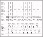
I'm sure the digipot wants rising edge clocking, but I don't know if it idles high or low. Seems to be low given the middle diagram on page 15. My current, very "exploritory" code is:
Code:
setfreq k31 'helps see what's going on, but i've tried varying this
symbol cs = B.1 'chip select pin is tied high
high 0 ;experimenting with reset pin state (currently tied low)

'pause 1000
pulsout 2,200
pause 1              'got and LED on pin2 so I can see where I am in the program
pulsout 2,200
pause 10

hspisetup spimode00, spislow    'trying the different modes, only trying the 00 modes atm
gosub Send_data
'hspisetup spimode01, spifast
'gosub Send_data
'hspisetup spimode10, spifast
'gosub Send_data
'hspisetup spimode11, spifast
'gosub Send_data
hspisetup spimode00e, spislow
gosub Send_data
'hspisetup spimode01e, spifast
'gosub Send_data
'hspisetup spimode10e, spifast
'gosub Send_data
'hspisetup spimode11e, spifast
'gosub Send_data
end

Send_data:
low cs ; enable chip select
hspiout (%1000000000) ; data
'pause 100
high cs ; disable chip select
hspisetup OFF
pulsout 2,200
'pause 1000
return
I've got my multimeter connected to the wiper and end terminal of RDAC 3 so A1=1 & A0=0 (page 18). I'm trying to send the data of zero so I think it should be %1000000000.

I also don't understand the 3rd diagram on page 15. I think I understand that the information it's trying to convey is that which I need, but I don't understand it.

Appologies if I've missed anything. Did some searching for spi stuff, but there's an aweful lot, and one thing I did pickup were some cases where the part to be interface with had picky requirements. I hope that isn't the case with this.

It would be great if a few of my unknowns could be confirmed one way or the other so that I can narrow down on specific problems. I could have made a mistake in my circuitry (breadboard) of course, but I've been at it for the day, checking and double checking and haven't had a single response. I'd really appriciate any advice.


Thanks in advance as always,
David.
 

westaust55

Moderator
Unfortunately, the datasheet seems to give no indication about how the "RES" pin is used (just try searching "res" or "reset").
From datasheet Table 4:
RES/AD1 == RESET in SPI Mode. Device Address Bit 1 in I2C Mode.
It is active low (as determined by the bar/line over the letters RES in the datasheet, so when low the chip is reset. Would normally use a pull-up resistor and then if you wish you can uae the PICAXE to pull/drive low when a reset is required.

And at page 18:
During reset (RES), the wiper is set to midscale. Note that unlike SHDN, when the part is taken out of reset, the wiper remains at midscale and does not revert to its pre-reset setting.
The HSPI hardware based on recollection (from past reading of datasheet only dealing with whole bytes of data.
Backed up by PICAXE manual 2 for HSPIOUT
Syntax:
HSPIOUT (data, {,data,...})
- Data is a constant/variable of the byte data to output
The chips needs 10 bits of data as 2 channel address bits followed by 8 data/setting bits.

I recommend that you first try to get the code working using the SHIFTOUT command (inbuilt for the X1 and X2 parts).

So instead of:
hspiout (%1000000000) ; data​

use:
Code:
SYMBOL channel = b6  ; range 0 to 3
SYMBOL setting =  b7 ; range 0 to 255

channel = 2 << 6   ; need to get the channel into top 2 bits of byte for MSB_First
setting = 128

SHIFTOUT <clk_pin>, <data_pin>,  MSBFirst_L, (channel/2, setting/8)
I leave it to you to define output pins for <clk_pin> and <data_pin>.
 
Last edited:

alband

Senior Member
It is active low (as determined by the bar/line over the letters RES in the datasheet
THAT'S what I was missing. Thank you. I'd found the other bits on it but without knowing that, they still didn't tell whether it should be high or low. Great bit of info in general too, bar = active low. I'll give my code a run with a pull-UP instead, just in case, then change and try the shiftout stuff.

Thanks very much westy! :)
 

alband

Senior Member
That's great! Got the code working this morning:
Code:
setfreq m4 'helps see what's going on, but i've tried varying this
symbol cs = B.1 'chip select pin is tied high
SYMBOL channel = b6  ; range 0 to 3
SYMBOL setting =  b7 ; range 0 to 255

channel = 2 << 6   ; need to get the channel into top 2 bits of byte for MSB_First
setting = 0

high 0 ;experimenting with reset pin state (currently tied low)

pause 1000
pulsout 2,200
pause 200              'got and LED on pin2 so I can see where I am in the program
pulsout 2,200
pause 1000

main:
readadc 2,setting
gosub Send_data
goto main

Send_data:
low cs ; enable chip select
spiout 3, 4, 1, (channel/2, setting/8)
high cs ; disable chip select
pulsout 2,200
return
The manual says that the shiftin/out commands aren't very efficient though. In the end product, I'm probably going to be short on time and trying to update three of these digipots very quickly (so I don't miss transmissions to/from a xbee). Could there still be any way of making it work with hspiin/out?
The end design would been on a different chip that needs to be decided upon, if that helps.

The digipot also understands i2C, but that's likely to be even slower than shiftin/out, isn't it?

Thanks for the help westy! Now I can start prototyping with this chip at least :D

David.
 

westaust55

Moderator
In i2c mode, the PICAXE will send two complete bytes of data for each channel setting. One byte for set-up data and the second for the actual pot setting (see DigPot datasheet page 16).

In General SPI is capable of faster data transfer rates than i2c at the &#8220;FAST&#8221; rate.

From the datasheet in SPI mode,
Note that only the last 10 bits that are clocked into the register are latched into the decoder.
Therefore it would seem that if you send two full bytes of data and have the channel address in the lowest two bits of the first bytes, the first 6 bits are in effect ignored.
Try (untested) the following approach &#8211; after the hspisetup of course:
Code:
SYMBOL channel = b6  ; range 0 to 3
SYMBOL setting =  b7 ; range 0 to 255

channel = 2 << 6   ; need to get the channel into top 2 bits of byte for MSB_First
setting = 128

hspiout (channel, setting)
 

alband

Senior Member
Got it! Had some problems though. First off, I think it would have to be "channel = 1 << 6". It would ignore bits0-6, then receive the "1" in A1 then the "0" in A0.
However, it appears that hspiout send it's stuff MSB first. It worked when I set "channel =%00000010.

Also, regarding which spimode to use: It works with all the modes except spimode01 and spimode01e, curiously. Any ideas why this is? The e on the end seems to make no difference at all. I'm surprised that modes other than 00 worked though.

My working code is now:
Code:
setfreq m4 'helps see what's going on, but i've tried varying this
symbol cs = B.1 'chip select pin is tied high
SYMBOL channel = b0  ; range 0 to 3
SYMBOL setting =  b1 ; range 0 to 255

channel = %00000010 '2 << 6   ; need to get the channel into top 2 bits of byte for MSB_First
setting = %00000000

high 0 ;experimenting with reset pin state (currently tied low)
hspisetup spimode00, spifast

'pause 1000
'pulsout 2,200
'pause 200              'got and LED on pin2 so I can see where I am in the program
'pulsout 2,200
'pause 1000

main:
readadc 2,setting
'sertxd (#setting,CR,LF)
gosub Send_data
goto main


Send_data:
low cs ; enable chip select
hspiout (channel, setting)
high cs ; disable chip select
return
Thanks for the help as usual, I really appriciate it!

David.
 

westaust55

Moderator
Sorry, my error there. :mad:
I knew the channel number was now to be in the two lowest bits but after cut and paste from my earlier example forgot to remove the <<6 which moved the channel to the two upper bits.
 

alband

Senior Member
No worries about the channel number. Without that error I wouldn't understand it as well as I do know :) Besides, you've solved my problem without even having the circuits in front of you, so I'm still well impressed :p

If the modes are solely related to the HSPIIN, then it's odd that a couple of them doesn't work for the HSPIOUT. Either way, I've got 6 other modes that do work and I shouldn't be needing any HSPIIN's.

I'm now just testing whether I can use two of the 8-bit pots in parallel, and stagger their valules to achive one 9-bit pot. Seems to work, though I used readadc 10 to get feedback of the pot value (terminals of the pot at the rails). The number kept fluctuating a lot even when the pot's were on a fixed value with no serial coms. I checked the voltage with my multimeter and found it was constant to within a milivolt. Is it expected that the readacd10 would vary by about 2 LSB each way?

Anyway, time for the 10-bit version with all four pots!

Thanks again :)
David.
 

alband

Senior Member
Thanks Westy, really useful documentm now in my HDD. Not sure I follow the bit about SMP though:
It must be maintained clear for any PICmicro device that is a slave. When in master
mode it will control whether data is sampled when the PICmicro MCU is in the
middle of sending its own data or whether the data is sampled when the PICmicro
device is at the end of sending its data.
Does that mean the master device will "look" for incomming data either while it's sending data or once it's sent some data? Both seem a little odd with respect to PICAXE given a command has to be coded for the PICAXE to "look" for incomming SPI data (or is it read at other times too and buffered somewhere?). Also, I can't imagine either PICmicro or PICAXE actually receiveing data while sending it?

Thanks for all the help!
David.
 

hippy

Ex-Staff (retired)
Thanks Westy, really useful documentm now in my HDD. Not sure I follow the bit about SMP though:
Unfortunately the quote from the slide presentation notes isn't as clear as it could be; the reality of what is going on is clearer in the timing charts of PICmicro data sheets.

SMP determines when, with respect to the SCK clock signal, each incoming data bit is sampled when receiving data from an SPI device.

Also, I can't imagine either PICmicro or PICAXE actually receiveing data while sending it
SPI can ( and actually does ) send and receive its data simultaneously; as 8-bits are clocked out, 8-bits are clocked in. However the PICAXE commands are only intended to support one or the other; clocking 8-bits out or clocking 8-bits in. Simultaneous send and receive can however be achieved by using HSPIOUT and a PEEKSFR to obtain what was clocked in after 8-bits are clocked out, and of course that can also be achieved by bit-banging SPI.

Many SPI setups and operations only require data to be clocked out or data to be clocked in, but some devices do receive and also send data, some may send this simultaneously ( sending as they receive ) and others may do this in separate phases of operation.

Some SPI devices ( SD Cards for example ) may actually be quite complicated, receiving data, then sending a reply to that previous data while receiving the next data. This increases data throughput rates but makes the control software side of things more complicated.
 

alband

Senior Member
Interesting. Is there a particular reason why there's no dedicated command for doing in and out at the same time? Would the PEEKSFR method be just as fast/efficient as such a hypothetical command? I've not yet "done" PEEKing or POKEing but I've read the PEEKSFR description and think I understand it (essentially allows a user to read some variables deep inside the chip?). Does that mean that any time HSPIOUT is issued, the chip also samples the "hspi sdi" pin? And when data HSPIIN is issued, the chip effectively "sends" %00000000?

I'm a bit confuse then as to the purpose of CKE and SMP.
I get CKP, it dictates whether the clock should idle high or low to communicate with a particular device.
CKE stands for &#8220;Clock Edge Select&#8221;.
The exact function of CKE will depend on the setting of CKP, which we will look at
later. In the meantime, know that this bit controls when data is transmitted when
compared with the clock.
So does this tell the PICmicro when the device it is comunicating with EXPECTS the data to be sampled relative to the clock (so, does the device expect to sample the bits on a rising or falling edge?).
SMP determines when, with respect to the SCK clock signal, each incoming data bit is sampled when receiving data from an SPI device.
And so is SMP the same as CKE except that it tells the PICmirco when IT should expect to sample the data relative to the clock. To summerize, do SMP and CKE represent the same thing, but for the different cases of data being sent and received from the PICmicro?

Thanks for the replies
David.
 

hippy

Ex-Staff (retired)
Interesting. Is there a particular reason why there's no dedicated command for doing in and out at the same time?
Most SPI use for PICAXE users would be SPI output only or SPI input only, or using devices which expect SPI sent and then deliver SPI results back, so the commands fit that.

If one sends and receives SPI at the same time one could only do it a byte at a time. It's possible to have such a command which does that and that it doesn't exist is probably because there was no need seen for it, and it can be achieved using existing commands anyway.

Does that mean that any time HSPIOUT is issued, the chip also samples the "hspi sdi" pin? And when data HSPIIN is issued, the chip effectively "sends" %00000000?
Yes, would be the short answer but it can be a bit more complicated than that.

I'm a bit confuse then as to the purpose of CKE and SMP. I get CKP,
You need to look at the PICmicro datasheet timing diagram which makes it clearer (attached).

CKP and CKE set one of four clocking schemes which set polarity of the clock pulse and define when the data is output and stable with respective to the rising / falling edges of the clock pulse.

SMP determines when the data back from the device is sampled.
 

Attachments

alband

Senior Member
I'm a firm believer in "if it ain't broke..." so, yeah, I'd agree with that.

Yes, would be the short answer but it can be a bit more complicated than that.
I won't ask further then, especially as it's just curiosity and wont actually help anyone. Thanks for the answer though.

Re the diagram, that does make things a lot clearer, thank you. As always, great to have a forum where the "technical support" are happy to help a curious mind!

Thanks again,
David.
 
Top