Soldering
- Thread starter Svejk
- Start date
hand soldered?
Congrats if it is!
Some small packages like that (if your lucky) have the pads exposed on the outer edge of the chip making it possible albeit difficult to solder.
I myself have recently purchased a Gordak 952 2 in 1 solder station off Aliexpress from a chinese supplier, cost me £55 inc P&P and is an awesome bit of kit. Would make jobs like that heaps easier!
IronJungle
Senior Member
Nice job. I couldn't do that in my wildest dreams. (Of course my wildest dreams don't often include soldering, but you get my drift....)
mrburnette
Senior Member
@Svejk.... do you hire your eyes and steady hands out? I had to click on the image to see what the blue blur represented! Old eyes and shaky hands...Maybe a bit off topic but I'm too excited not to share.
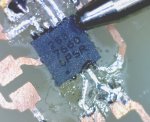
DFN10, 3x3 mm package. Etched and soldered. Pictured with the tip of a fine ball pen.
View attachment 10696
- Ray
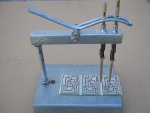
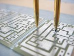
As more components are only becoming available in smd packages we need to adapt to work with these tiny packages.
A few years back i threw together a gadget to assist in the placement of smd packages, it helps out on those days where the fine motor skills are on the shaky side.
It allows me to take time with the tweezers to align the component correctly over the foot print, more important when working with the tiny IC's with fine little pins.
Then i can solder the component with a fine tipped soldering iron easy.
The back pin holds the PCB steady while the front pin holds the component in place during soldering.
With pressing the lever the front pin lifts first to allow the back pin to hold the board while the chip is positioned, fully pressing the lever lifts both pins.
cravenhaven
Senior Member
Thats a clever little device SABORN.
mrburnette
Senior Member
Yes, SAborn, that is one smart device.

- Ray
Perhaps "evolution" will evolve humans into creatures that can easily see and work with the microscopic (I use a stereo zoom microscope personally, surplus eBay)As more components are only becoming available in smd packages we need to adapt to work with these tiny packages.
- Ray
Thanks for replies.
Actually it wasn't that hard. Once etched (I had 8 mil between pads of DFN package) I just placed some soldering paste on pads and I heated the copper traces without touching the die. About 10 seconds later I've had it done. I've used 2 mm chiesel tip and the iron was set at 300ºC.
@Stan, it is just an accelerometer that I need to use to aquire some data. I could wait 3 weeks to have it done professionally or have a go at it.
@Ray: you need to ease on that coffee, look at your eyes