I'd like to bounce this off you guys to obtain suggestions for improving the circuit. Doing stuff like this solo makes you wonder what could be better.
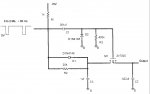
Attached is a simple capture and hold circuit to convert a PWM input signal into an analog value for a PicAxe A/D input. The object is to provide fast response to PWM input signals, while the 08M manages a concurrent PWM out with HI and LOW commands. The 08M basically measures the input values, does maths for the hi and low output pulse times and performs the output pulses. With this circuit there is no delay waiting for the latest input pulse width value.
Have this is running on a 08M with 2 pole low pass filters. The filters cause a trade off between faster response and a lot of ripple and output jitter, or to slow response and less jitter.
In an effort to obtain faster more stable response this circuit was worked up on an old Microsim simulator, until it operates more or less as expected.
When the input goes low, the voltage on C3 ramps down until the rising edge of the pulse occurs. At that point M1 conducts and transfers the voltage to C2. C1 provides a short pulse to the gate of M1 allowing M1 to conduct briefly.
One concern is with the MOSFET M1, it was about the only one with a model that worked in simulations. Surely there are other transistors that would be more suitable. Suggestions appreciated. Two circuits will be needed for the application, so a dual package would be handy. Any other comments and suggestions appreciated.
Attachments
-
 56.3 KB Views: 51