PICAXE based Logic IC Tester

westaust55

Moderator
As a follow on from my recent 14M based Logic probe here
I have now started work on a PICAXe based Digital/Logic IC Tester using a 28X2.

Inspiration came from the bundle of 74HCxxx TTL and a few 4xxx series logic IC's I have many form a recent fire-sale buy at Dick Smith.

At the moment, the program is restricted to testing the basic NAND, NOR, AND, OR, XOR, etc gates in 2, 3,4 and 8 input formats ,for 74HCxxx chips but as the code occupies just under 2 kBytes in a chip (28X2) with 4 x 4 kBytes slots there is plenty of room for program expansion.

One area I will shortly change is from the 16x 2 LCD (currently using an AXE033) to a 24x2 LCd module which will allow presentation of more details.

Over the next few posts I will provide some details for others who may be interested.

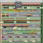
Attached here are the PEBBLE layout for the main board and the ZIF socket board
 

Attachments

  • Logic IC Tester Main Board June2011 .JPG
    Logic IC Tester Main Board June2011 .JPG
    401.5 KB · Views: 194
  • ZIF Socket for 18pin use.jpg
    ZIF Socket for 18pin use.jpg
    210.1 KB · Views: 123
Last edited:
PICAXE 28X2 based Logic IC Tester

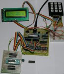
Attached are some photos of the main board and pheripheral parts (LCD, ZIF socket, keypad).

Don't worry about the breadboard, that is just used as a connection point for power an intermediate connections until I build the circuit into an Altronics sloping front plastic case (shortly)
 

Attachments

  • Logic IC Tester 01.jpg
    Logic IC Tester 01.jpg
    235.8 KB · Views: 160
  • Logic Tester 16x2 Displays.jpg
    Logic Tester 16x2 Displays.jpg
    249.1 KB · Views: 145
Last edited:
PICAXE 28X2 based Logic IC Tester

Attached is the PICAXE 28X2 program code thus far.
Once I have a 24x2 LCD display working this will be advanced further but it is sufficient to prove operation of the hardware and verify simple logic gate based IC's as it stands.
 

Attachments

Last edited:
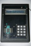
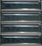
Finally, I have a couple of photos of the complete project in a plastic case with the 2x24 Char LCD module.

Hmm, on looking at the photos, I realise that I had still not removed the protective plastic strip over the LCD display
 

Attachments

  • ICTester2.JPG
    ICTester2.JPG
    250.2 KB · Views: 94
  • Tester_Screens.jpg
    Tester_Screens.jpg
    252.6 KB · Views: 87
Last edited:
PICAXE 28X2 based Logic IC Tester

The first attached file is the schematic diagram for the main controller board (minus filtering and decoupling capacitors - see PEBBLE layout if you want clues for these :) )

EDIT:
The schematic diagram for the User Interface (keypad and LCD) circuit and the ZIF-18 socket has been added as sheet 2 below.
The "Custom" header socket strips shown in the schematic (and photos) on both sides of the ZIF-18 socket allows the User to patch the power supply for IC's under test which do not use one of the 4 automatic power supply configurations.
 

Attachments

Last edited:
Absolutely excellent and a brilliantly neat idea.

If you want to go to insane extremes you could do it like a cable tester, generate all possible input combinations to a chip and read all outputs back, working out which are inputs and which are outputs and determining the chip type ! Probably over-kill when you know the type of chip and simply want to know if it works or not.

One extension and alternative to a larger text display could be a GLCD or cheaper 'Nokia knock-off' which could show the package, the gate layout inside, and even show which pins are duff.
 
Thanks hippy.

I have used the Nokia type gLCD in the form of the slightly higher resolution (101x64) from the Siemens A55 and similar mobile/cell phones in the past (older thread by me on the forum for that topic).
Albeit quite clear, maybe in my case at least (now where are those specs) getting a bit small on the overall size for presentation of data in a quick and readable format.

Do have some more conventional 128 x 64 resolution gLCDs to hand and maybe a Mark II could go that way.

With the larger 24x2 text LCD (and something similar could be achieved with 16 or 20 x 4) I figure that during testing process I can put the IC ID/type, No of logic gate under test and test No on the top line and then along the second line have the gate No (1 to 8 to cover up to octal devices (eg 74HC240/245) followed by an alpha character (-= untested, T=test in progress, F=fail and P=pass, so as the tests progress keep a progressing record as for example:
Code:
[B][[/B]74123 Gate:7 Test 6/8   [B]][/B]
[B][[/B]1P 2P 3F 4P 5P 6P 7T 8- [B]][/B]
Which will fit on the 24 char wide text display but only indicates logic gates/blocks not individual pins.


Although may not be obvious for some until I post the schematic (soon *) the keypad is a 4x3 with ressitors and data entry is via a single ADC input.
Most logic chips are 14, 16 or 24 pin plus a few at 28 pin.
ZIF sockets to hand are 18 pin and had figured out a way to transfer a data signal to pin 1 of the ZIF-18 with pwr to pin 18 but then checks reveal there are virtually no 18 logic pin devices to consider other than microcontroller.

* Rather contradictory that here 'we' are always asking the newcomers to post their schematic so we can help them fault find,
yet I tend to "draw" the schematic in my mind, look at the pinout and construct a prototype (with no faults of course :cool: ) then prepare the schematic only for future reference in case I do need to come back to it after the Alzheimers has set in :eek:.


Moral: Newcomers - please do as I say and not as I do :)
 
Last edited:
in the footsteps of Nikola Tesla, but he failed to produce the documentation before his sad demise and the world lost the details of a lot of technology as a result

So by my estimation that puts you one up on Niloly, what a guy . . .. :)
 
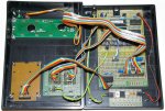
In additon to the photos just added at post 5, here is a photo of the internals.

The ribbon wiring is somewhat messy due to leaving them long enough to easily open the casing (in case the need arises at a future date).
 

Attachments

  • IC Tester Internals.jpg
    IC Tester Internals.jpg
    264.3 KB · Views: 91
Albeit far from complete, attached are some initial words as a manual of sorts for the 28X2 based Digital Logic IC Tester.
Posting this now as it may be a while reaching completion and just looking at the program code alone will not make it clear where the IC is installed in the ZIF socket and how the header sockets are used.

EDIT: 26 Sept 2011:
A few more pages added in Rev B to further describe operation.
 

Attachments

Last edited:
My friend can you send me one simulation of this project with any simulator ?
This is my graduation project please help me ...
Many Thanks to you ...
 
Welcome to the PICAXE forum.

I am not quite sure exactly what you seek when you state "can you send me one simulation of this project with any simulator?"
I have not emulated or designed the project in any simulation package such as VMS or SPICE.


The project as presented here is a fully working hardware project.
With the project, I have provided here on the forum some basic software.

However, I am not prepared to provide a complete solution to enable anyone to copy a 100% complete project to pass their studies.
This is because, as stated in the manual as written and posted above:
A full compliment of software has not been included with the project as it is known that such
a project is often assigned to classes at secondary and tertiary education institutions
. The
software as posted for this project is limited to a range of basic AND, NAND, OR, NOR, NOT (inverter) and XOR logic gates.

I trust that you understand my position on this matter.
 
I feel very humbled!

Thanks for the inspiration! I have my keypad working with 2 digit numbers, and that is all I need for now. I can see how I can add more fairly easily. I just tell a variable to add 1 each time a key is pushed - and that is how it knows how many digits have been pushed. Very simple stuff :)

Printing the rest of my arm now!

Thanks for your help good people! ^^
 
Back
Top