pcb and picaxe

magnustullock

New Member
Hi,
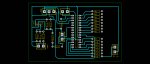
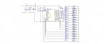
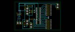
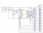
Have been using straight tracked circuit boards till now with a ton on soldered wires. However I now want to try to tidy all that up with a designed PCB. I am using design spark and have included the pickaxe libraries. I have added the 28x1 chip as well as the resistors required but the tracks are running between the pickaxe pins (will upload an image later). Can anyone confirm this is ok for a pickaxe circuit to have tracks this close? will tracks that close to pins not suffer from cross talk or electric noise? Are there any recommended settings in terms of track and pad width for design spark to make it more suitable for picaxe?

Thanks
Magnus

tracks.jpg
 
Last edited:

geoff07

Senior Member
I expect it would work, but note:

a) the tracks could be re-arranged by hand to simplify the routing, and

b) the main issue is: how will it be fabricated? If professionally, then I'm sure it can be made, though at a price. If at home, then much depends on your method.

With a good sharp exposure, fresh developer, fresh etchant and careful monitoring, it could be done. The risk is that tracks bleed or undercut and you get shorts or breaks.

By the way, if you are doing it yourself, a laser print onto plain paper, made translucent with olive oil on the back, is very effective with 50% longer exposure time, at low cost. Just make sure you wash the oil off the board before developing.
 

Dippy

Moderator
I take it this is an Auto-routed (or A/R + tinker) board?
The tightness of track-track and track-pad (Fire pad) looks like Mr Auto-router has been at work.


Is this PCB going to be professionally made or home-made?
I only ask as some tight clearances can be a problem if the home-maker is new to it.

Tracks running between pads isn't ideal but often OK - it depends on the circuit function.
For high frequency / high impedance / sensitive designs it can be a total NO-NO as you could suffer the effects you mention...and more.

Many CADs allow you to 'neck' (narrow) tracks between pads to give a little more clearance.
Very thin tracks/traces can be a problem with home-made boards unless you have good gear and follow the more traditional methods of manufacture/

IN some cases move the component to prevent track going between pads.
It certainly looks like you can.
Remember: with PCB design you get points for functionality NOT artistic merit :)
If you can combine both then well done.

Generally, where possible I would increase track-track clearance and make tracks wider.
Also, if this is a prototype board and where space permits, I'd move resistor IDs to the side so that you can read them after the component is inserted.
 

MartinM57

Moderator
Also, and it might apply in this case or not, you can sometimes re-arrange the schematic to be more PCB friendly i.e. make the PICAXE pins go to the resistors right next to them, rather than having to go round the houses - and then compensate for the layout in the software by adjusting input/output pins to suit
 

Paix

Senior Member
As Dippy has said, with larger clearances between tracks and beefier tracks, even Mr Autorouter won't be tempted to route tracks between your pins.

It seems to be a bit of a universal truth that autorouting does an extremely complex job and not always for the best. You probably have a fair idea of what things should look like, so place your main components for best effect and drag the others about to achieve a balance of it being logical and looking passably pretty. Most people I think would tend to advise against auto routing as it's likely to make life more, rather than less difficult in the short term.

It does look like a very nice compact board before you start to consider the difficulties that it brings to the table. I still have to properly get to grips with DesignSpark, so good on you getting there.
 

Goeytex

Senior Member
Commercial products with traces between pins are very common. These are engineered products and I assume the engineers have considered the effects. However there are situations where it is not a good idea. However, if you get the board commercially made and there are no signals over about 1MHz it will probably be OK.

But, for your first board I would vote against it unless a few mm of extra space is a big deal. I would also suggest using a flooded ground plane if practical.
 

hippy

Ex-Staff (retired)
It's always worth looking at a commercial board for comparison, such as a PICAXE project board.

Tracks between pads should not normally be a problem in a low-speed circuit but if the board is manufactured without solder resist they can make soldering much harder. There may also be places where that is not appropriate.

Most double-sided boards I have seem to have thicker tracks and greater spacing between tracks. Usually three tracks max running up the body of a 0.3" pitch IC, so I would guess your track width and spacing could do with being doubled.

As noted; if you can lay out connectors and connections differently that can save a lot of routing. The top right routing seems to be because you are outputting 0-7 with connector order going 7-0. If you can match the connector order to the PICAXE pin order then most of that routing will disappear, tracks should become straight links from pins to adjacent resistors.

It can also help to start with a bigger board or greater spacing between component blocks as that can increase the number of options the auto-router will have.

As with anything, skills will increase the more you do. Unless one has a particular aptitude for the task the first results may never be as perfect or as ideal as one might like. That's a simple fact of life.
 

magnustullock

New Member
Many thanks for all the answers! It is an led chaser sequence for a "laser gun", which is designed to start on a switch. There is an interrupt pin on C.07 to initiate another sequence for the firing. To keep costs down I am going to try the board myself using the ironing method (I assume the olive oil trick works with this?).

I am a little unsure. I have put on a 9v -> 5v regulator on as in the manual, but my previous project had a regulator with 2 capacitors only which seems to work well, is the recommended one mandatory?

I am also unsure of how to add a 20 pin ribbon housing onto the board with design spark. But getting there slowly.

gun3.jpg
 

neiltechspec

Senior Member
Can't see any capacitors at all on your pcb.

You must add the recommended 0.1 on the PIC power pins and a couple around the regulator.

If it was me, I would make the Gnd (0v) track a lot thicker as well.

Neil.
 

magnustullock

New Member
thanks Neil, I am happy enough with solder prototype boards. However, I am just hacking about with this at the moment :) all advice is very welcomely received!
 

Buzby

Senior Member
Please post the circuit diagram. We can then see where to make any improvements. You are nearly there !.
 

Dippy

Moderator
"...capacitors are not exactly the same values..."
There's often a degree of flexibility with values depending on app and arrangement BUT your first 'port of call' should be the manufacturer's data sheet for guidance on values and types. Generally speaking, where there are variants on a device, check the data sheet rather than verbatim copying of circuits from websites... including Forums.

Anyway, moving on, as said by Buzby a schematic may help others to provide you with tips and advice.
 

SAborn

Senior Member
The oil and paper trick is one i have used for over 10 years, but it only works with photoresist board, not iron transfer.

I might be a little old fashioned, but i see a board as a sheet of copper and only try to remove the minimum copper i can leaving the greater part of copper as tracks and pads etc.

Your circuit design has bees whisker tracks and fine pads, which is a good recipe for a disaster on a home brew board, why remove all that copper and leave a bees whisker remaining, when all you really need to remove is the copper between each track/pad to give a clean break.

For a development board its best to leave as much copper as able, as fine pads with fine tracks will just break away when you go to desolder a component.

In your circuit R1 to R15 go nowhere, you forgot to add a pads to connect each resistor to.

My view with home made boards is, have a go, you wont be sorry you tried, but the golden rule is you can always remove copper later if needed, but you can never put it back.
 

eclectic

Moderator
A couple of thoughts.

Will all programming be away from the board?

If so, connect Serial In to ground?

ADC0 / ADC1. Resistors to Gnd?

e
 

magnustullock

New Member
A couple of thoughts.

Will all programming be away from the board?

If so, connect Serial In to ground?

ADC0 / ADC1. Resistors to Gnd?

e
Thanks eclectic, I wasnt aware of the need for a resistor between the switch/ADC 0/1 and ground. What sort of ohms would that be roughly do you think?
 

Paix

Senior Member
. . . I am going to try the board myself using the ironing method (I assume the olive oil trick works with this?).
Alas, NO! The point of using oil on paper is to render it translucent, in order to use a photographic development system.

For the iron on technique, you ideally need a thin(?) glossy paper, (out of a magazine?) which you are able to use in a laser printer without difficulty and which will come apart easily when wet. The object being to transfer the toner from the paper onto the board. Sticking firmly followed by careful paper removal through soaking and very light abrasion, with fingers. The board itself has to be very clean, so oil would be a total disaster in that scenario.
 

Hemi345

Senior Member
Does Designspark have a ground pour or polygon option? Try that for your ground connections, that will allow you to keep a lot more copper on the board which means less time etching and potentially undercutting of the traces. Beef up the traces to at least 16-24mil, that's totally possible for most on that board. I see a lot of traces looping around and between pads that are unnecessary if you use a ground pour. If no ground pour option, look at tying traces together using the shortest route possible. For example, combine the two traces running up the center of the 28X1 into one big track and link the trace that winds around next to "INT" and tie it to that big track.

On a few boards that I made using the toner transfer method, I had a laminator so it made the 'ironing' process easier. I printed my design on a full color ad from a photography magazine. The glossy'er the page, the better. Clean the copper side of the board many times with acetone till a white cloth stays white. Then taped one side of paper to the board and ran it through the laminator tape first till not only was the toner 'stuck' to the board but also the paper itself. Then put the board and boiling water in a bowl and let it sit for about 5-10 minutes. Basically when the water is comfortable to touch, the paper should slough off gently with your finger. You should not have to peel on it or scrape with your finger. If it doesn't come off this easily, boil some more water and soak it for another 5 minutes.

Example with beefy traces and ground pour using toner transfer method before etching:
 

Attachments

Hemi345

Senior Member
Yes, the ground pour will basically "flood" all the spaces on the board not occupied by other signals connecting all the ground connections together. I highlighted the ground connections in blue so you can see how they're all connected.

The yellow part I highlighted is an "orphan". I would recommend turning the "allow orphans" option on (if DesignSpark has that option) so that even though that island of copper provides no connection, it won't require extra etching time to remove it.

Also it's helpful to use thermals, the little 'cross looking' connections where a pin will be soldered to the ground pour. Without thermals, the ground pour will act like a heatsink and make soldering of those locations difficult.
 

Attachments

magnustullock

New Member
ok, here is my "final prototype" . Can anyone see major issues? points to note:
-Serial In is tied to ground as the download will be done on a breadboard
-Ground flood will replace the ground track
-capacitors between power pins and either side of regulator
-each LED (tip and blink) have resistors
-still cant figure out how to get a shrouded/unshrouded connector for the 15 resistors to connect to
-each switch (INT, SW1) have resistors between them and the pin as well as ground
-INT will cause and interrupt on C.7 and also cause TIP to light up

gun5.jpg

apart from the things mentioned above can anyone see anything glaringly wrong here?

many many thanks and if I ever meet any one you then the first drink is on me! :)
 
Last edited:

JimPerry

Senior Member
Personally I'd put a diode in the + supply, before the regulator. Stops everything releasing "magic smoke" if connected to AC or back-to-front by mistake :rolleyes:
 

MartinM57

Moderator
With no circuit diagram to compare it with, or no integrated schematic->PCB integrity check (if Design Spark does that) it will always be a bit of a guessing game whether you have made any mistakes or not, or whether the circuit is fundamentally adequate (e.g. I see no 100nF decoupling capacitor close to the PICAXE) .

I would suggest:

- adding the two download resistors and a plug (3x 0.1" pins, or the standard 3.5mm stereo socket) - you will quickly get highly irritated having to remove/replace the PICAXE to program it

- simplify all those traces with unnecessary wiggles - straight traces are much more reliable for DIY boards - eg the LH side of R1-R4, R6-R8, R14 etc

- an old teacher always told me never to have right angles when turning 90 degrees - use a 45 degree "mitre" to get round the bend (it's all to do with possible track undercutting on the inside of a 90 degree bend). The "T-junctions" you have under the PICAXE are OK (in fact the right angle bend under the PICAXE is how I would have them all)...
...and make the mitres as long as possible, so the overall track lengths are minimised

- always go into a circular pad at right angles (normally at 0, 45, 90, 135, 180, 225, 270 or 315 degrees using compass headings) - you're OK apart from the pad to the right of R26, top of R27...

- make most of the tracks much thicker so there's less chance of any etching problems - 40 thou/1mm or so as a default absolute minimum width, probably more like 2mm would be good - you've got them all at the width that passes between the PICAXE pins

- show the ground plane on the picture - so we should be looking at something like Hemi's photo
 

inglewoodpete

Senior Member
I noticed that resistors 2 to 15 all solder into the board but don't have a place for an external connection. Is that what you intended?
 

hippy

Ex-Staff (retired)
The circuits around SW1 / Tip / INT seem wrong to me but without a circuit diagram I cannot tell what was intended.
 
Last edited:

srnet

Senior Member
And another reason for making tracks as thick as you can is that, especially on single sided boards, if you need to remove a component, there is less chance of the pad lifting and damaging the track during a repair.
 

hippy

Ex-Staff (retired)
Also, a rather fatal flaw in not having any power supply going to the chip. Leg 20 connects to C3 + but neither connect to a power rail.
 

magnustullock

New Member
I noticed that resistors 2 to 15 all solder into the board but don't have a place for an external connection. Is that what you intended?

Hi, that is something which I referred to earlier, I cant seem to find a suitable shrouded/unshrouded header in design spark to add so that all resistors can then be sent to a bargraph on a different board (space reasons).

cheers
 

magnustullock

New Member
Also, a rather fatal flaw in not having any power supply going to the chip. Leg 20 connects to C3 + but neither connect to a power rail.
oops haha. yes well spotted! theat was there, but I think I removed it when I was tinkering! that may indeed cause some issues lol
 

magnustullock

New Member
it may also be pretty poor, but this is the schematic that I came up withDesign1.jpg

Thats strange, the ground to the LEDs (the detached bargraph) has been chopped off, but it is there in the schematic
 

hippy

Ex-Staff (retired)
it may also be pretty poor, but this is the schematic that I came up withView attachment 16014
The schematic does not match the layout. R17 and R18 are on the circuit but not in the layout, R23 and R24 are in the layout but not on the schematic, there are other inconsistencies.

On the layout the N/O and N/C contacts of SW1 are shorted together where they should not be according to the schematic. There are other shorts to those points which do not appear in schematic. Whatever "Tip" is on the layout does not appear to be on the schematic.
 

magnustullock

New Member
The schematic does not match the layout. R17 and R18 are on the circuit but not in the layout, R23 and R24 are in the layout but not on the schematic, there are other inconsistencies.

On the layout the N/O and N/C contacts of SW1 are shorted together where they should not be according to the schematic. There are other shorts to those points which do not appear in schematic. Whatever "Tip" is on the layout does not appear to be on the schematic.
sorry my bad - at work and have accidetally posted an old version. will post the correct one from home later
 

hippy

Ex-Staff (retired)
sorry my bad - at work and have accidetally posted an old version. will post the correct one from home later
It happens, but I think the important thing beyond matching schematic to layout, is the layout isn't right.

If that's not a result of schematic error, then something is going wrong in the schematic to layout conversion process.
 
Top