PC board fabs
- Thread starter julianE
- Start date
Interesting, as I found the DipTrace schematic function to work well when I designed a fairly large board (40X2, UMFPU, maybe a half-dozen smaller chips, dozen or so off-board connectors [GPS, among other things]) several years ago It came in just under the DipTrace "free" limit of xxx pins ;-) Something I designed for a friend and he wasn't interested in checking my work on the PCB. I did have to cut one trace and add a jumper wire but that could have been avoided with another set of eyes :-( However, all the features did work, which is as good as PCB design gets.I sent in my second board, it was a struggle to get it under 100mm. Turns out as soon as it's larger than 100mm there is a $4 "engineering fee" and the board prices go up as well. Being on the cheap side of thrifty I spent an hour rearranging components to shrink the board to 99mm.
5 boards for around $10 delivered.
I'm not sure how others do it but I find drawing a schematic in diptrace a waste of time. The way the program arranges the components on the board is a jumble that takes too long to untangle. I find it easier to have a printout of the schematic and arrange the components manually in the PCBLayout window. I also waste a lot of time looking for components, I needed a JFET with the middle pin being the gate, took a while to find one.
I'm guessing it will all get easier with use. I'll start working on the next board, it's nice having a sample board for figuring out spacing of components.
It absolutely does work and if I was designing professionally I would follow the suggested method. I can see making a large board how having a schematic in diptrace would be beneficial but for my piddly little boards I plan on drawing a schematic on paper and then going straight to layout.( However, all the features did work, which is as good as PCB design gets.
Maybe I'll change my mind if there are a lot of errors with the board I sent out today, it's an analog circuit with two jfet transistors.
It's funny once one retires you'd think time would hang heavy, for me it's the opposite, i'm always short on time and take shortcuts if at all possible.
good grief, you must have valuable skills to have gone out of retirement so often.I'm retired for the 4th (or is it 5th) time. Some days are just too short to get done what I want done. Maybe part of that is being OLD ;-)
Totally off topic, but an answer to your question.
My last few years with my long term employer (30+ years), I was part of the software "skunkworks" team that fixed the things that "can't be fixed" - preferably wth no hardware cost. That was mostly a process of seeing what other people could not see.
Example: A software support organization tells the users' manager there's no way to determine how long it takes to process a request for service. That continues for two years until my boss asks me "Can you get this guy off my back?"
I ask for a read-only ID on that data system and just browse through the data tables. It appears that every action has a date/time stamp so I put together a quick and dirty prototype in Excel (good place to extract data and do math on dates and times) . The users' manager saw it running and said "I want that on my desk today!" No changing to a logical layout, no cleaning up of all the cells displayed to just leave those of interest. Ugly, naked data was all he needed.
After I retired from that job (retirement #1) that manager called me at home and asked "How much to make a 'work from home' version? He paid that out of his own pocket.
I went back to university to finish a degree (strictly for personal satisfaction) but was interrupted the first semester back by another division of my original company that needed a "Can you fix that?" person.
After graduation, I worked as an independent programmer for several years, working with startups in two states in the US (some Palm development; some Windows) and some translating from subject matter expert words to computer terms for web development for the US military.
Just fixing what "can't be fixed" ;-)
Thanks for sharing, fascinating career. I'm sure most everyone on this board has an interesting story to tell, it's hands down the most interesting corner of the internet. No matter how oddball a topic I come up with an expert advice is posted tout suite.Totally off topic, but an answer to your question.
My career is nowhere as colorful, got a good job right out of college and stayed there 30 years.
I received my second board and it's a beauty, soldered the components and the preamp sounds great. I need to start on the next project.
I have all these projects in need of nice enclosure. Has anyone a recommendation for a service to make 3D printed enclosures, I know JLCPBC offers 3d printing service, anyone try it.
I have all these projects in need of nice enclosure. Has anyone a recommendation for a service to make 3D printed enclosures, I know JLCPBC offers 3d printing service, anyone try it.
i'm guessing metal printing is very expensive. i found an example of a smart phone size plastic project enclosure and i think it was $40.metal 3D printing
i'd like to get a home 3d printer but it takes up goodly amount of space and seems very fiddly. i'm also hearing it takes hours to make a print.
3D printing can be time consuming. The bigger the item - the more plastic to be included - the longer it takes. Be aware that an "open" item may have internal supports that are just to support the upper portion until the print job is completed - that printing puts down more plastic and takes more time and you have to remove the supports ("falsework" for bridge builders) when the item is completed.
.
.
The variances in printing go beyond size, info density and amount of support network needed.
There is a common test print called the benchy. It normally takes about an hour to an hour and a half to print. But a well setup printer will do it less. A decent core xy or Delta have been know to do it in less than 10 minutes.
As for space, it depends how big a print volume you want. There is an open source printer that fits inside a filament spool box.
Fiddling, yeah can be until you get the thing setup just right and then it just works.
rq3
Senior Member
I've had several small parts CNC machined from aluminum by hubs.com. In quantities of 5, they cost about $60 each. JLCPCB will print them in stainless steel for $8 each. I'm tempted, despite the weight.i'm guessing metal printing is very expensive. i found an example of a smart phone size plastic project enclosure and i think it was $40.
i'd like to get a home 3d printer but it takes up goodly amount of space and seems very fiddly. i'm also hearing it takes hours to make a print.
hubs com is new to me, good website, they had a sample part about 110mm cube, $63 printed in nylon, not unreasonable for a custom made part delivered in a week or so.hubs.com
$8 for a small metal part is a bargain.I've had several small parts CNC machined from aluminum by hubs.com. In quantities of 5, they cost about $60 each. JLCPCB will print them in stainless steel for $8 each
i've been making enclosures from plexiglass or perspex for our international friends, it's pretty easy to work with but not terribly attractive.
I've considered 3d printed enclosures in the past. I just checked jlcpcb prices to have a useful enclosure (https://grabcad.com/library/enclosure-for-digital-electronic-part-tester-pcb-1 - approx 65mm x 75mm x 20mm) printed.
The cost (excluding shipping and taxes) would be about £2.70 for white plastic resin and about £65 for 316L stainless steel. So that's not bad really for the plastic one.
Personally I've never really liked the look of 3d printed enclosures. I find the 'acrylic sandwich' construction (acrylic sheets are the bread, the pcb is the filling and is held in place with hexagonal pcb spacers) within even my limited construction abilities; they'd be no good in the rain though.
I like this idea from Allycat: avoid actually having an enclosure
I'm interested to hear of others experiences with 3d printing or making enclosures generally, I always find them hard to get right

rq3
Senior Member
Here are descriptions of somewhat incestuous enclosures and circuits (the 3D printer is printing parts for itself). But they do use Picaxes. In one case, the enclosure had to be opaque. In the other, it had to be translucent.I've considered 3d printed enclosures in the past. I just checked jlcpcb prices to have a useful enclosure (https://grabcad.com/library/enclosure-for-digital-electronic-part-tester-pcb-1 - approx 65mm x 75mm x 20mm) printed.
The cost (excluding shipping and taxes) would be about £2.70 for white plastic resin and about £65 for 316L stainless steel. So that's not bad really for the plastic one.
Personally I've never really liked the look of 3d printed enclosures. I find the 'acrylic sandwich' construction (acrylic sheets are the bread, the pcb is the filling and is held in place with hexagonal pcb spacers) within even my limited construction abilities; they'd be no good in the rain though.
I like this idea from Allycat: avoid actually having an enclosure
I'm interested to hear of others experiences with 3d printing or making enclosures generally, I always find them hard to get right
Attachments
-
285.5 KB Views: 5
i have made acrylic boxes using acrylic adhesive and it's not too difficult, the issue i run into is making the opening for displays, tough to get right. i have a new portable dremel tool and a bit for cutting acrylic i will have to give it a try this weekend and yea i like the acrylic sandwich method. most every other project is either open like alan's or enclosed in big shrinkwrap sleeve.find the 'acrylic sandwich' construction (acrylic sheets are the bread, the pcb is the filling and is held in place with hexagonal pcb spacers) within even my limited construction abilities; they'd be no good in the rain though.
The price for the enclosure you posted is very reasonable, what would be the easiest to learn package for making files that JLCPCB needs to fabricate?
been at least 10 years since I used a CAD program.
Well, I went and ordered a couple nextion faceplates, got the stl files from one of the sharing sites. I also downloaded FreeCad, I have used autocad a long time ago, back when you typed in coordinates, will go through tutorials on using freecad.
my thinking as far as enclosures is just to print the faceplate, the box itself is easy enough to make. price for 2.4" and 3.5" nextion display faceplates is couple dollars, very inexpensive. i have made boxes out of aluminum before and the faceplate was always the most difficult part, I'll look into how much an aluminum faceplate would cost.
my thinking as far as enclosures is just to print the faceplate, the box itself is easy enough to make. price for 2.4" and 3.5" nextion display faceplates is couple dollars, very inexpensive. i have made boxes out of aluminum before and the faceplate was always the most difficult part, I'll look into how much an aluminum faceplate would cost.
Do you have any tips for cutting acrylic for the boxes? I don't have a bandsaw so I score the sheet, snap it and then sand the edges.i have made acrylic boxes using acrylic adhesive and it's not too difficult
I agree, openings are the toughest part for me. I bought a drill press (and can finally get my holes square to the board) and attempted milling openings with it: I got poor results, my slots tend to wander off to one side. I now print the opening dimensions on paper, glue it to the acrylic, cut the opening with a coping saw and then tidy up the edges with a file.the issue i run into is making the opening for displays, tough to get right
I don't know which is easiest but I use Freecad because it's open source and has plenty of tutorials on youtube (I am slowly working through a series from a channel called Adventures in Creation). I don't find cad modelling particularly easy but I do enjoy the process.what would be the easiest to learn package for making files that JLCPCB needs to fabricate
Did you order these from jlcpcb? Once again, I'm interested to hear how they turn out.Well, I went and ordered a couple nextion faceplates
Something I have considered doing is to get part of the enclosure (perhaps the faceplate) made out of a pcb since FR4 board is pretty strong. I have used jlcpcb to make a technical ruler before (screen printed with useful formulae, constants, pcb trace widths, drill hole sizes) and also a key ring. Openings could probably be defined by drawing the appropriate shape and moving it to the 'edge cuts' layer, I think people have slots milled on a board in this way. It's easy then to put text and graphics on the front silk layer in one colour. Other text/graphics can be put on a front copper layer: that subtly shows through the soldermask, or you can also copy the design to the soldermask so you see solder-coloured text/graphics.
With regards to cutting openings for displays and buttons, I now have a few approaches.
The first method is to draw any slots, holes or openings on the PCB layer and have the PCB house cut the slots for me. I've drawn the PCB for my Grid Frequency Meter and positioned the LCD on the 'inside' of the board so that it is visible through the slot, the picture of this (on the blue mat) shows the front (unfilled) and back (filled) of the PCB. This gives a reasonable finish, especially when the dimensions of the board is matched to fit an existing case, with slots in it such as the range from Hammond Enclosures. This exposes the soldering though, making it visible, but for simple projects this isn't an issue and having the hole neat and square is far better than anything I could do with drills and a file.
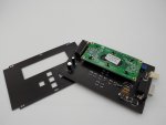
The second approach is to create the first PCB, with the LCD again positioned on the rear, visible through a slot. Then make a second PCB with no components on it at all, with slots cut into it which match the position of the LCD and any buttons. This is what I did for a work project, where I have five buttons arranged in a cross type position which can be pressed through openings in the upper PCB. Again these are dimensioned so that the upper PCB fits into the uppermost slot of a Hammond aluminium enclosure, with the lower PCB in the slot directly beneath it. I even drew two PCBs to make up the end plates of the case which have holes cut into them for the D-Sub connectors, their stand offs and a further connector all matching the main PCB so that they align up when they are screwed together. This looks very professional once assembled.
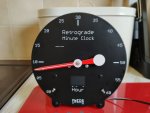
For LED seven segment displays, these can be hidden behind a suitable array of small drilled holes. If they are positioned close enough together this forms a grid which, with the LED display pressed tightly up behind, it allows the LEDs to shine through when lit, but almost invisible when off. The grid is just visible above the word 'Hours' on the Retrograde Clock, behind this is a two digit seven segment LED display. The red 'hand' for this clock is another PCB, with the hole placed in the correct location for screwing to the servo motor shaft. Behind the main clock 'face' PCB is the main board which has the display mounted on it on the 'front' of the board, with the LCD and control buttons on the 'back'. This is mounted with spacers and positioned so that it forms a stand to allow the clock to be freestanding.
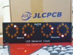
For individual LEDs, simply draw appropriate holes on a second PCB and mount it above the main one. If the holes have a plating it makes them look really neat. The Dekatron Clock has three PCBs, one as the front panel with holes to let the LEDs shine through, one below with the LEDs and drivers and one with the LCD, time keeping chip and processor made up as BogBean suggested 'sandwich' style with spacers. No prizes for guessing where the PCBs were made...
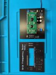
The first method is to draw any slots, holes or openings on the PCB layer and have the PCB house cut the slots for me. I've drawn the PCB for my Grid Frequency Meter and positioned the LCD on the 'inside' of the board so that it is visible through the slot, the picture of this (on the blue mat) shows the front (unfilled) and back (filled) of the PCB. This gives a reasonable finish, especially when the dimensions of the board is matched to fit an existing case, with slots in it such as the range from Hammond Enclosures. This exposes the soldering though, making it visible, but for simple projects this isn't an issue and having the hole neat and square is far better than anything I could do with drills and a file.
The second approach is to create the first PCB, with the LCD again positioned on the rear, visible through a slot. Then make a second PCB with no components on it at all, with slots cut into it which match the position of the LCD and any buttons. This is what I did for a work project, where I have five buttons arranged in a cross type position which can be pressed through openings in the upper PCB. Again these are dimensioned so that the upper PCB fits into the uppermost slot of a Hammond aluminium enclosure, with the lower PCB in the slot directly beneath it. I even drew two PCBs to make up the end plates of the case which have holes cut into them for the D-Sub connectors, their stand offs and a further connector all matching the main PCB so that they align up when they are screwed together. This looks very professional once assembled.
For LED seven segment displays, these can be hidden behind a suitable array of small drilled holes. If they are positioned close enough together this forms a grid which, with the LED display pressed tightly up behind, it allows the LEDs to shine through when lit, but almost invisible when off. The grid is just visible above the word 'Hours' on the Retrograde Clock, behind this is a two digit seven segment LED display. The red 'hand' for this clock is another PCB, with the hole placed in the correct location for screwing to the servo motor shaft. Behind the main clock 'face' PCB is the main board which has the display mounted on it on the 'front' of the board, with the LCD and control buttons on the 'back'. This is mounted with spacers and positioned so that it forms a stand to allow the clock to be freestanding.
For individual LEDs, simply draw appropriate holes on a second PCB and mount it above the main one. If the holes have a plating it makes them look really neat. The Dekatron Clock has three PCBs, one as the front panel with holes to let the LEDs shine through, one below with the LEDs and drivers and one with the LCD, time keeping chip and processor made up as BogBean suggested 'sandwich' style with spacers. No prizes for guessing where the PCBs were made...
Last edited:
I use a table saw with a carbide blade. Woodworking a hobby that i sadly neglect due to all the dust that interferes with my other hobbiesDo you have any tips for cutting acrylic for the boxes?
")
I have a goodly amount of tools but cutting openings in acrylic is a pain, i've used a scroll saw which does a nice job but it's never perfectly straight at least not for me. I'll look for the fluted bit that i got for cutting acrylic with a dremel tool. My thinking is if i can set up some sort of a guide for dremel to follow it might work.
Freecad is good but like everything these days, highly complicated and bloated. I'm trying to learn just enough to make boxes.I use Freecad because it's open source and has plenty of tutorials
I wish someone would distill million and one options in freecad to a simple box software, put in the dimensions and voila, nice box with a lid.
I think it can be done with macros so eventually it could become simple.
Yes, ordered from jlcpcb and i will write an update once it comes in. so far, it seems to take a bit longer than pc boards. i'm still waiting for the files to be approved, looks like a human looks at it before it's put into production and it's done on business days so probably on a weekday. good to see that people get a weekend off in china. i have seen pc boards used as front panels , it's a good idea.Did you order these from jlcpcb? Once again, I'm interested to hear how they turn out.
Well done, clocks look great, love the keep it simple approach.With regards to cutting openings for displays and buttons, I now have a few approaches.
I've seen videos explaining the parametric approach to customise generic enclosures, e.g. this oneI wish someone would distill million and one options in freecad to a simple box software, put in the dimensions and voila, nice box with a lid.
I think it can be done with macros so eventually it could become simple.
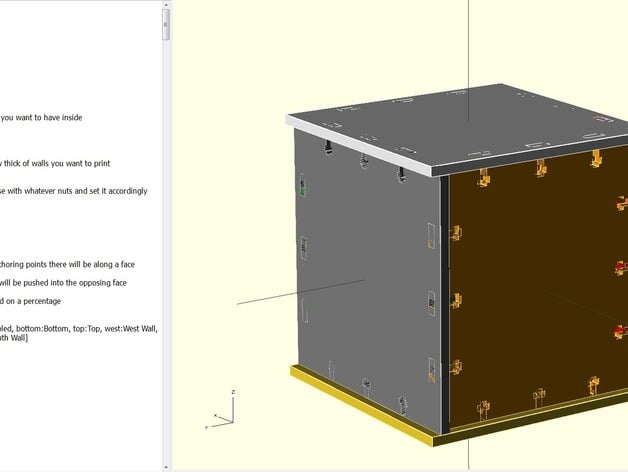
I wondered if it could help. I find it easier to learn a new software package when there's already a model to tinker with, rather than generating something from scratch. I expect many other parametric enclosure designs can be found, this example just happens to be available in freecad quite easily on github: https://github.com/SensorsIot/Project-Box-Templates/blob/master/ParaBox-5-1.FCStd
The model is rapidly customizable (in dimensions but not in the features present) by tweaking values on the spreadsheet
Thanks for posting your methods, they are very neat, I'm inspired to try them. One question: did you just draw the outline of the shape for the openings on the 'cuts' layer or does it need to be a filled polygon? Or perhaps it does not matter.With regards to cutting openings for displays and buttons, I now have a few approaches.
i do have a router, safest way to get it done is to rout the cutouts on a large sheet of plexi and then cut with the table saw. i hesitate using a router on a small piece of plexi, it would work well with a jig.probably have a router
i like the guy with the swiss accent. i'm also liking tinkercad, it's meant for classroom. good enough for me.'ve seen videos explaining the parametric approach to customise generic enclosures, e.g. this one
Another option is OpenSCAD, which allows you to use code to define a project. Here's are some box makers on Thingiverse:
 www.thingiverse.com
 www.thingiverse.com
Search Thingiverse for "box maker" to find more.
OpenSCAD is here:

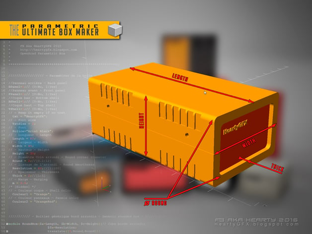
The Ultimate box maker by Heartman
The file include now the Panel Maker. this project... My first try with OpenScad, the box is fully customizable. I hope you will enjoy with it, and will show us many boxes made with. If you play with the Fillet value you will go from the sharp to the round sides box If you want a chanfered box...
Parametric Box maker by savorywatt
T-slot based case generator. You specify what size object you want it to surround and your material width and it makes a printable box with slots for you to use screws to put it together. The github version allows you to export a file you can cut with a laser.
Search Thingiverse for "box maker" to find more.
OpenSCAD is here:
OpenSCAD
openscad.org
I "draw" them on the dimension layer in Eagle as a rectangle. For slots I have sometimes added them to the slots and milling layer(s). I might also write a note in text within the area I'm expecting to be cut out saying some thing like "This is a rectangular hole, 133mm x 35mm" just in case. Never had one come back without the holes yet. The Gerber viewer on JLCPCB often doesn't show the cut outs which is why I often add my notes just to give me an extra level of confidence.Thanks for posting your methods, they are very neat, I'm inspired to try them. One question: did you just draw the outline of the shape for the openings on the 'cuts' layer or does it need to be a filled polygon? Or perhaps it does not matter.
rq3
Senior Member
Me too. I bit the bullet and ordered the $8 stainless steel part from an existing STEP file last week. In on-line chat just now, they indicated that the file has been sent to the engineer for review, but it's early morning there. From what I know of Chinese New Year, he may not be in a condition to review much of anything. No problem, no hurry. I used the same STEP file for ordering CNC'd parts, so I have confidence in its accuracy.my 3d prints are still in "File Review" stage. Maybe it's because of Chinese New Year, it's taking far longer than PC board fabrication.
They should have an option to skip the review, just ship me what I ordered, I want to see and compare the consequences. $8 is in the noise. $11.37 including shipping to Maine, which is about as antipodal as you can get.
EDIT: I had to check. The antipodal point from my house in in the middle of the ocean, off the west coast of Australia.
Last edited:
my opposite point is in French land, Kerguelen Islands, middle of nowhere.The antipodal point from my house in in the middle of the ocean, off the west coast of Australia.
mine is still being looked over too, my guess, the engineers are all coming back from their hometowns and they only have a skeleton crew working.
I suspect that the reveiw is to determine the best orientation to print out taking into account did like the amount of support material. It may also be where the file is sourced and turned into g code resulting to be sent to the printer. So no skipping the reveiw I'm afraid.
I have read on line of people having their designs rejected.
My project is in production, had something odd happen, I prepaid with paypal when i submitted the files and yet my order status this morning stated "awaiting payment", checked my emails and i had not been charged so i went and paid. It's in production now. I'm guessing they wait to charge paypal until it's in production and there is a timeout with paypal but who knows maybe i'll get double charged.
My project is in production, had something odd happen, I prepaid with paypal when i submitted the files and yet my order status this morning stated "awaiting payment", checked my emails and i had not been charged so i went and paid. It's in production now. I'm guessing they wait to charge paypal until it's in production and there is a timeout with paypal but who knows maybe i'll get double charged.
rq3
Senior Member
In my case, they did flag an area that effectively goes to a sharp edge and is probably not printable, but is machinable. The edge is not important, and I authorized the print. It will be interesting to see what I get. I've had no issues printing the part in various plastics, but 316 stainless steel, no!I suspect that the reveiw is to determine the best orientation to print out taking into account did like the amount of support material. It may also be where the file is sourced and turned into g code resulting to be sent to the printer. So no skipping the reveiw I'm afraid.
Hemi345
Senior Member
I used to use waterproof enclosures quite a bit for my projects, especially the ones with the clear lids so I could see status LEDs or displays (plus I like to show off the PCBs I've designed.
Here's my Humidistat project in one:

And my coldframe controller:
 drive.google.com
But in the last couple of years, I've been designing and 3D printing enclosures for various projects. Like Oracacle said, once you get the 3D printer dialed in, then it just works. Filaments with a matte finish hide layer lines really well and playing around with the print orientation, some of my designs don't look 3D printed at all.
Here's my Humidistat project in one:
And my coldframe controller:
20180325_141722.jpg
drive.google.com
But in the last couple of years, I've been designing and 3D printing enclosures for various projects. Like Oracacle said, once you get the 3D printer dialed in, then it just works. Filaments with a matte finish hide layer lines really well and playing around with the print orientation, some of my designs don't look 3D printed at all.
The bear
Senior Member
Aries
New Member
They look like the cable glands such as this https://cpc.farnell.com/pro-power/mg-20-white/m20-cable-gland-white/dp/CBBR7375?st=cable glands that I use quite often in my outdoor or garage projects. I'm quite keen on the tiny M8 ones as well.What are those white screw-on (and I assume waterproof) connectors
Hemi345
Senior Member
Cable glands, as others have said. They have a silicone bushing inside that when the cap on the gland is tightened, squeezes around the wires and provides a water resistant barrier. Figured it was somewhat important since the inside of the cold frame can get pretty humid so trying to keep the electronics as moisture free as I can. It's been running none stop for almost 5 years and working well.Nice-looking. What are those white screw-on (and I assume waterproof) connectors you have going into the 2nd box?