MAX6955 slave address?

Jaden

Senior Member
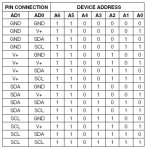
Ok I am having a go at driving some seven segment displays with a MAX6955. I amusing it because it uses the i2c bus and is common cathode, it ticks all the boxes I have! Now I have been able to run a SAA1064 chip successfully but it is a new learning curve with the max chip. Below is the adress for the SAA1064 chip, how do I find the address for the max chip? I have looked through the document on the max chip and could not find it (blind in one eye and can't see out the other posibly).


Code:
Symbol disp = %01110000						'display address
Symbol dispcode = %01000111					'instruction byte
Thanks
 

SAborn

Senior Member
Blimy you are blind.
A link to a data sheet is always good to save us having to find one.

As per the data sheet..........

Slave Address
The MAX6955 has a 7-bit-long slave address (Figure
4). The eighth bit following the 7-bit slave address is the
R/W bit. It is low for a write command, high for a read
command.
The first 3 bits (MSBs) of the MAX6955 slave address
are always 110. Slave address bits A3, A2, A1, and A0
are selected by the address input pins AD1 and AD0.
These two input pins can be connected to GND, V+,
SDA, or SCL. The MAX6955 has 16 possible slave
addresses (Table 5) and therefore a maximum of 16
MAX6955 devices can share the same interface.
And then there is a full list of the addresses on page 10.

http://www.datasheetcatalog.org/datasheet/maxim/MAX6955.pdf
 

Jaden

Senior Member
Thanks, just needed to look at it a few times! So I have %1101110. if I tie AD0 to SDA & AD1 to AD1, nice! Just had to decipher it.

Thanks
 
Last edited:

SAborn

Senior Member
If it was me i would tie the AD1 and AD0 pins to ground and make the address 11000000, thats if that address is not use for another device on the bus.

You did pop your glasses on and seen this chart of addresses in the data sheet didnt you.

I2C Address.JPG
 

Jaden

Senior Member
Yep, but no but yep! I was looking elsewhere and read about table 5 but did not look at it! Blond moment.

I was thinking to tie them to SDA and SDL as this will be easier when it comes time to build the PCB and routing? My circuit pretty much is one picaxe controlling the max6955, so if it does not upset the rotation of the earth as much as todays date (little mayan joke there) then I will keep them on SDA & SDL, or is this going to effect my program.... Which leads meonto the next bit..... I have been using the SAA1064 through the i2c bus with I think your and others help, well now that I am onto a different chip (needed a common cathode driver, and have ordered chip). And once agian I am bogged, Below is what I have, I know I need to read the chip data but am Iin the right direction?
Always trying to find a quicker path to enlightenment.

Code:
Symbol disp = %1101110					      'display address of max6955, see table 5
Symbol dispcode = %01000111				      'instruction byte


Symbol d1 = b0							'first Segment
Symbol d2 = b1							'second segment
Symbol d3 = b2							'third segment
Symbol d4 = b3							'fourth segment

							'
Symbol H = %11011001
Symbol E = %11110100
Symbol L = %10110000
Symbol P = %11010111

Let d1 = H
Let d2 = E
Let d3 = L
Let d4 = P

i2cslave disp,i2cslow,i2cbyte
Main:
	writei2c 0,(dispcode,d1,d2,d3,d4)
	goto main
Thnaks
 

SAborn

Senior Member
Just had a quick look and Disp = %1101110 is missing the zero off the end (8 bits not 7 bits) = %11011100

And by memory this line is wrong .... writei2c 0,(dispcode,d1,d2,d3,d4)
The 0, should be inside the brackets i think .......... writei2c (0, dispcode,d1,d2,d3,d4)
Also the HELP will need to be put into a lookup table.
 

hippy

Ex-Staff (retired)
I was thinking to tie them to SDA and SDL as this will be easier when it comes time to build the PCB and routing?
I was surprised to see tying to SDA and/or SCL suggested in the datasheet. It's probably valid but will potentially add all manner of confusion and doubt and I'd recommend tying to 0V ( and/or +V ).
 

Jaden

Senior Member
Thanks SAborn, I was trying to start simple as my countdown routine does use the lookup tabel. I was not sure anout the 8 bits it mentioned, so thanks. The 0 outside the brackets does work for the SAA chip but I will put it inside. I will give it a go and see if I can work the rest out. I am just getting confused because it has 16 outputs and I only need 8 and it uses a different segment adressing system. I will have agood read and get back when I get stuck....which could be soon.

Thanks
 

westaust55

Moderator
The 0 outside the brackets does work for the SAA chip but I will put it inside.
The SAA1064 requires a starting register address which you would be trying to achieve with the zero outside the brackets. It can equally be placed inside the brackets as per my example here:
http://www.picaxeforum.co.uk/showthread.php?22252-Getting-Started-with-the-SAA1064-i2c-bus-4-Digit-7-Segment-LED-driver-chip


For the MAX6955, the “address” is one term used in the datasheet for the byte wide "comamnd" register.
As the first byte sent in an i2c output program line is written to the “address”/command register whether that byte is before or inside the brackets will likely have no effect.

Both chips (SAA1064 and AMX6955) have an auto incrementing address/command register so after the address/command byte is sent, the first data byte sent in the same BASIC program statement is stored in the register which the command register points to. If more than 1 data byte follows, the command register is auto increments and the next data bytes are stores in subsequent consecutive registers.
 

inglewoodpete

Senior Member
I was surprised to see tying to SDA and/or SCL suggested in the datasheet. It's probably valid but will potentially add all manner of confusion and doubt and I'd recommend tying to 0V ( and/or +V ).
No it will almost certainly fail. The designer must select pull up or pull down for each address pin and then adhere to that addressing in the i2c parameters in PICAXE Basic.
 

westaust55

Moderator
No it will almost certainly fail. The designer must select pull up or pull down for each address pin and then adhere to that addressing in the i2c parameters in PICAXE Basic.
That may be jumping in at the "deep end" IWP.
The MAX6955 datasheet expressly covered connecting each of the two address pins to one of the following: V+, 0V, i2c SDa, or i2c SCl
to achieve 16 possible slave address from two inputs.
I do not disagree that it seems strange and I have not experimented with the MAX6955 but I am sure that Maxim have a working scheme.
The MAX6955 block diagram indicates the two address pins also conenct into the i2c controller but but little other information able how it works internally.
 

SAborn

Senior Member
I all ways say play it safe and tie the pins to Vdd or Vss, unless you need a different slave address, its the first I2C chip i have encountered where you can use the SCL and SDA as address pins, but they claim it works in the data sheet.

In many ways its a ingenious method.

Still the KISS method when using a new chip is where i always start and recommend.
 
Top