one of my next projects involves using a real time clock and an spi wireless module.
i will be running the project at 5v as from what i understand with the DS1307 is that it does not like less than 4v5 for the i2c comms to keep active.
however my rf module has a max Vin of 3.6v but from a look at the datasheet it says max vin on any digital input to be no more than 5v25, and digital input i would assume means the MOSI and CLK pins from the 40x2.
would i be correct in taking this to possibly mean the data pins are 5v tolerant?.
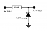
its not an issue if it would be safer to run it at say 3v3 which is below the max Vin but if that is the case then what option should i approach for the level conversion between the 40x2 and the rf inputs,presumably something similar to the level shifter that gets used with 5v mcu and 3v3 i2c.
initially i was going to power the project at 3v3 which would have worked for the rf module and have to admit i assumed the rtc chip would be fine with that voltage but after reading around a bit it seems it needs more juice to keep it happy.
to date i have not done any level shifting for devices communicating at different voltages so any reference diagrams or suggestions for parts i need to add to my end of month components splurge would be greatly appreciated,even better if i can keep it along the smd route as with the other board components.
thanks,
tony
View attachment DS-RF2400-NANO-V10-EN.pdf
i will be running the project at 5v as from what i understand with the DS1307 is that it does not like less than 4v5 for the i2c comms to keep active.
however my rf module has a max Vin of 3.6v but from a look at the datasheet it says max vin on any digital input to be no more than 5v25, and digital input i would assume means the MOSI and CLK pins from the 40x2.
would i be correct in taking this to possibly mean the data pins are 5v tolerant?.
its not an issue if it would be safer to run it at say 3v3 which is below the max Vin but if that is the case then what option should i approach for the level conversion between the 40x2 and the rf inputs,presumably something similar to the level shifter that gets used with 5v mcu and 3v3 i2c.
initially i was going to power the project at 3v3 which would have worked for the rf module and have to admit i assumed the rtc chip would be fine with that voltage but after reading around a bit it seems it needs more juice to keep it happy.
to date i have not done any level shifting for devices communicating at different voltages so any reference diagrams or suggestions for parts i need to add to my end of month components splurge would be greatly appreciated,even better if i can keep it along the smd route as with the other board components.
thanks,
tony
View attachment DS-RF2400-NANO-V10-EN.pdf