I2C Motor controller

100317

New Member
Hi Forum.

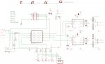
I found a circuit diagram of an engine driver with a Pic and L6203 on the I-net. I modified this circuit with a PICAXE18X.

I'm not an electronics expert.

Could somebody of you take a look on the circuit diagram, and say whether this is useful?

Any advice or corrections are very welcome.
 

Attachments

hippy

Technical Support
Staff member
I think you will have to better define how you mean by "useful".

It is not clear if you are using the 18X to control an I2C system or expecting the 18X to be controlled by I2C; only the 28X1 and 40X1 can be controlled as I2C devices.

Your connections to the 18X do not seem to be correct, particularly with respect to VDD and VSS; the pin numbering does not appear to match with the 18-pin PICAXE range.
 

westaust55

Moderator
Over and above hippy comments, is the component "DIGI" a socket or an IC?
If a socket what connects into the socket?
If an IC what exactly is it?

You need to give far more explanation about what you are proposing to do with the circuit.
 

100317

New Member
Basically I wanted to use the Picaxe18x to control 2 engines, however, has overlooked that he is not usable as a slave.

My mistake.

The Picaxe18x should be controlled by a 28X via I2C.

I have compared the Pin assignment once again with the pinout diagram in Manual 1 and have found no mistake.

DIGI is a socket, to control the 18X over I2C. On Pin 5 and Pin 7 are regulated +5VDC. Pin 9 has regulated +12VDC. Over Pin 10 serial communication with the master is possible.

Below in the circuit are 4 jumpers which can be connected to GND, if not in use. Otherwise these connections are planned for end position Switches.

In the circuit I use two mass lines (GND and GND1) which are connected over Pad0 and Pad1, because the lines for the engine control are very broad and I have found no other way to solve this.

Ok, I have to change the circuit diagram on a 28x1.

Thank you for your advices.

Hans
 

hippy

Technical Support
Staff member
I have compared the Pin assignment once again with the pinout diagram in Manual 1 and have found no mistake.
U1 shows -

5 VDD - connected to GND
14 VSS - connected to +5V via "DIGI"

VDD is the positive supply to the PICAXE ( not 0V ) and is on leg 14 ( not leg 5 ).

VSS is the 0V / GND supply ( not +V ) and is on leg 5 ( not leg 14 ).

Those are mistakes which could damage or destroy the PICAXE, the power supply and other components if it were powered-up.
 
Top