Help with current source circuit

GreenLeader

Senior Member
Hope everyone had a merry christmas... I certainly did.

Not exactly a PICAXE question, but I am looking for some help with a circuit to compensate for the 1G offset on the output of an accelerometer. The accelerometer produces about 1.3mA per G. The output is sensed by measuring the volt drop across a load resistor. (see circuit diagram attached)

The accelerometer design notes recommend the circuit shown in the attachment. This injects the desired -1.3mA to null out the 1.3mA accelerometer output.

Could anyone explain how it works and give some suggestions on component selection?
Many thanks
Steve
 

Attachments

premelec

Senior Member
The op amp "wants" its input between the + & - to be 0 so puts current through R2 to generate a voltage to offset the zener diode voltage at the other op amp input. Since the gate current is very small the drain current on the FET represents the current through R2 which by ohm's law is Vz/R2... in order to keep the op amp difference voltage at 0. I don't know if this circuit would work in your actual operation as there are various voltages to consider etc... looking at more data about the device being offset could find a simpler solution.

Usually with this type of situation I'd offset the output with the PICAXE program math... but analog electronics ain't dead yet!
 

John West

Senior Member
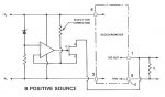
Here's a fairly complete analysis for you. You may want to read some of this twice. I can't describe things very clearly in text format. I'm more of a talker. I'd suggest you glance at a copy of the schematic as you read this. It will make more sense:

As Premelec indicated, the whole purpose of the circuit is to use an op-amp and driver FET to maintain a fixed current flowing through R2, (and to select that value of current by selecting the correct R2 value.) In this case, that's -1.3 mA. This is accomplished by a common bi-polar (+/- supply) single op-amp (such as a uA741, LM301, LM321, LF351, TL071) whose output will, in this circuit operating off the negative power supply rail, attempt to cause its inverting (-) input voltage to be driven to match the Zener reference voltage on its noninverting input (+).

It will do this by driving the FET (any small-signal common N channel FET will do, BS170, 2N7000, etc) so that it maintains a given voltage (that of the Zener,) across R2, which will thus have a fixed current flowing through it. The voltage drop across R2 will be forced by the op-amp and FET combination to be identical to the Zener reference voltage.

As far as component values are concerned, we must start with the Zener, as the voltage of the Zener you select will determine the other component values. Though others will certainly work, I'd suggest something like a common 1W 5.1V Zener (example: 1N4733A) for the voltage reference. Chose commonly available parts whenever you can in order to save money and avoid problems later on. If you don't already know what's commonly used, do a web search for something like "Zener diode," and see what pops up on the first page or two of results. (Or ask someone here.)

Then pick a value of R1 that will provide sufficient current to drive the Zener into its linear regulating range. (Check the Zener's data sheet.) Something like 10 mA should work (but check it, as that's a generalization for this example.) The lower the current that flows in the circuit the better as far as power conservation is concerned. However, the Zener must be driven hard enough to be certain it will stay within its linear regulation range during any load fluctuation. In this circuit, the choice of an appropriate resistor is made easy, as the op-amp input is the only load, and that is both negligible and doesn't fluctuate.

With a +/- power supply voltage differential of 30 volts, and a Zener diode drop of ~5 Volts, you have to drop 25V across R1. Ohm's Law then calculates an R1 value of 2.5K Ohm if you want 10 mA to flow through it and the Zener. (The op-amp will have negligible current flowing into its inputs.) Any value close to the 2.5K value will be fine. The Zener diodes are reasonably tolerant of input current range. Again, select the actual resistor value used based on the data sheet for the Zener you use.

With a 10 mA current flowing through a Zener diode that drops 5.1 volts, there will be a power dissipation of 50 mW (Ohm's Law for power; P=IE.) This is well within the diode's power spec of 1W dissipation.

Next comes the key component selection, that for which the circuit was designed.

For resistor R2 you must pick a value that will cause a 5.1 Volt drop when 1.3 mA of current flows through it. As we already know, the circuit is designed to force a 5.1V drop across R2. Therefore we must select it's resistance value to ensure that 1.3 mA is flowing through it when 5.1V is dropped across it. Ohm's Law again finds the correct resistor value. R=E/I. Resistance equals voltage divided by current. You can do the math.

As resistors are fixed values, in this case, if a precise -1.3 mA current flow is desired, a trimmer potentiometer may be necessary to get the correct resistance value. The bias nulling current will be off by the value selected for this resistor as well as the error caused by the inaccuracy of the actual Zener voltage. Also, any difference between the -1.3 mA offset specified as being required and the actual offset required for your particular accelerometer chip.

That component selection is clearly based on your choice of degree of bias current nulling precision for your application and (as Premelec mentioned,) the code you use. Bias current nulling precision may not be an issue in your application, as the schematic shows a fixed resistor for R2.

Note that for anything resembling violent accelerations, use of a trim pot is probably not a very good idea. If both precision and mechanical reliability are important, then consider using 2 resistors (in parallel or series) for the value of R2 in order to get a precise current flow, i.e. use a resistor value just under that desired, and another with a very small value (series,) or one with a value just over that desired and one with a very high value (parallel,) in order to get very close to the required total resistance value.

In addition to the actual resistance values, we must also select resistors based on their power handling (wattage) capacity. Use Ohm's Law for power (P=IE; power in watts equals current in amps times voltage dropped across the device,) to calculate the power dissipation of each resistor value selected for this circuit to ensure you use resistors rated for sufficient wattage dissipation. At this supply voltage, Zener ref resistor R1 may require careful attention to proper power sizing, depending on the actual drive current selected.

Assuming the circuit shown is appropriate for the accelerometer used, you will then have a negative 1.3 mA flowing through the R2 circuit to act as your bias offset nulling current.
 
Last edited:

hippy

Ex-Staff (retired)
The accelerometer design notes recommend the circuit shown in the attachment. This injects the desired -1.3mA to null out the 1.3mA accelerometer output.
Do you have details as to what this accelerometer chip is, links to the datasheets and application notes, so readers can see for themselves, get a feel for exactly how the device works and its requirements ?

I'd have thought a simple summing op-amp circuit, accelerometer to '+' input and the offset voltage/current to the '-', would have done the job, or, as also suggested, simply subtract a value from the READADC reading.

One question is, once you've subtracted the 1G offset; what happens and what will you do with negative-G ?
 

GreenLeader

Senior Member
Many thanks for the guidance from John West and Premelec, I found that very useful - I have started reading up on the suggested components so I can have a go at a breadboard circuit.

Hippy - the accelerometer is a QA700 servo accelerometer. A google search will turn up some info but no detailed datasheets. The accelerometer is typically set up with a load resistor to produce 5V/G but I am interested in the dynamic part of the signal which is very low level, maybe 10mG or 50mV. So I want to null out the 5V DC part so I can make better use of the dynamic range of the ADC (which is a commercial data logger, rather than a Picaxe), ie I can set up the logger to receive +/-100mV input rather than +/-10V.
 

premelec

Senior Member
@hippy with folks attaching PICAXEs to motorcycles, automobiles, aeroplanes and submersibles why not to a paltry $1K accelerometer? I notice the device noise level is around 3mg. At the price I would be inspired to study the construction of accelerometers... It's not stated what the absolute accuracy, response time, stability and repeatability needed are and that's likely where the pricey figure comes in. [on the other hand maybe it's only because it's aimed at government agencies] I thought we had a lot of cheap MEMS inertial sense devices available now - removable from your air bag system and powered with a battery from an unused [currently] smoke detector.
 

GreenLeader

Senior Member
Here's a fairly complete analysis for you... .
Thanks John that is really helpful. The zener and R1 are going to add about 300mW to the power draw compared to the circuit without compensation, which is still within the capacity of the power supply I've selected, so thats OK.

I looked at teh zener spec sheets but I couldn't readily identify the current at which they are in their linear range. On one of them there was a graph that seemed to be linear from about 10mA upward, so maybe 10mA is at the bottom of the range.

To take things a bit further, supposing I needed to do the compensation in the opposite direction, ie reverse the current direction? The design notes show a similar circuit - attached - but it seems to have a different type of FET (a P-channel) if my googling has been accurate:).
My local electronics store carries the 2N7000 N-channel FET you suggested, but it does not seem to carry any P-channel FETs. Is my interpretation correct or can I use the same FET, just with a re-arranged circuit?

Ideally I'd like to build a circuit that I can switch between positive and negative offset compensation (to cater for mounting the accelerometer vertical up or vertical down) or no compensation.

I was thinking of doing this with a switch to have the option of (1) no compensation (2) positive compensaion, (3) negative compensation. I'd need a 6-pole 3-position switch, which are scarce. If I can use the same FET then I can get a away with fewer poles.

Or is there a better way?

Many thanks
Steve
 

Attachments

premelec

Senior Member
There are voltage references which would take far less power and be more stable than the zener setup... To change the current bias you can switch the current sense resistor or the bias voltage or use a voltage divider off the current sense resistor. All of these would only require an SP3T switch... study the circuit further till you can sense what it's up too :)
 

premelec

Senior Member
I'll second that Martin - the LM317 is fine and cheap - and you can use it with a fixed resistor on the reference side of the op amp and just vary the current from the 317 with a switch for changing ranges...
 

GreenLeader

Senior Member
Thanks guys,
I am currently (corny pun) going down the mosfet/op-amp path. I got lost with Premelec's suggestion of using a LM317 with an op-amp as I thought the LM317 would replace the op-amp and FET? (I don't have an electronics background to draw on so I am in the follow-the-explicit-instructions mode to a large degree).

I have built the circuit using a TL071 op-amp and 2N7000 FET and tested it on a 1k load (do not want to hook up that expensive accelerometer until I am a bit more confident). It all worked rather nicely and I got very close to my 1.3mA without trying very hard to select precise R values, so many thanks John West for that great explanation.

My next step is to find a P-channel FET. I think a ZVP3306A will do the job, on the basis of comparing to BS170/2N7000 specs, but I'd appreciate it if anyone could confirm or offer an alternate?
The specs for the 3306A are:
Current Id Max:-160mA
Drain Source Voltage Vds:60V
On State Resistance:14ohm
Rds(on) Test Voltage Vgs:-10V
Voltage Vgs Max:-20V
Power Dissipation:0.625W

I have managed to find a 4P3T switch, so I could use two of these to switch from the positive to negative current source. A bit clumsy but should work.

PS - the TL071 op-amp has two offset pins, which I don't think I need to use - how should I terminate them - is it safe to leave them floating?

many thanks
Steve
 
Last edited:

MartinM57

Moderator
http://www.eleccircuit.com/current-source-with-lm317/ (not brilliantly written and a couple of typos, but good enough. Look at that LMGTFY link above for others)

Just select an R value so that 1.25 (volts)/R (ohms)= constant current (amps).

So for 1.3mA (0.0013A), R = 1.25/0.0013 = 961 ohms.

And that's all you need - no other components at all.

As the current is so low you can use a multi-turn trimpot as the R (but you couldn't if you were looking at say 500mA constant current) and adjust it to get exactly the (small) current you need.

Use an LM337 in the same configuration for negative constant current.
 
Last edited:

GreenLeader

Senior Member
Just select an R value so that 1.25 (volts)/R (ohms)= constant current (amps).

So for 1.3mA (0.0013A), R = 1.25/0.0013 = 961 ohms.

And that's all you need - no other components at all.
Thanks MartinM57 - two questions:
  1. Is 961 ohms acceptable for an LM317? The data sheet seems to suggest that R must be less than 120 ohms, ie current must be >10mA. (see extract from data sheet)
  2. I sketched up what I think you are suggesting (attached): swap between a LM317 and LM337 depending on whether I want + or - current.
 

Attachments

MartinM57

Moderator
Interesting - hadn't seen that bit in the data sheet :(

The 120R gives 10mA constant current so that you're into the 10ma>Iout>Imax that the rest of the data sheet is applicable to.

However, I've just set a 1K trimpot to 961R (Fluke DVM, but no idea how accurate ;)), breadboarded it onto a LM317T just as the data sheet and measured the constant current out.....1.31mA - effectively exactly as predicted.

Whether this could be claimed as operating "out of spec" for the LM317 is a bit debatable - you couldn't rely on the rest of the parameters in the data sheet so things like temperature stability (not mentioned in this thread so far - is it an issue?) might be a problem, but it does appear to work fine.

YMMV, but it's very simple....
 

MartinM57

Moderator
...the alternative would be to get the LM317 to deliver 10mA (i.e. in spec), but have another circuit that draws 8.7mA leaving the rest for your device. A LED maybe...or a constant current consuming circuit - but they tend to be a bit complex.
 

premelec

Senior Member
LM334 current source

One of the problems with electronic design is - so many choices! It looks to me like the LM334 IC would be good for your application - it only goes _up to_ 10 ma and is made for regulation of small currents... get the data sheet at www.nsc.com . Note that an extra diode and resistor need to be added for zero temperature coefficient use... [Fig 3 page 6 on my data sheet]. The TO-92 LM317 unit might have a lower current output limit specified. Note that with a two terminal current assembly you just need to get polarity on these 2 terminals right so you can use a 'positive' regulator to pull toward negative by putting it to a negative supply on it's negative terminal -
 
Top