External Resonator
- Thread starter ckalkhof
- Start date
PICAXE Manual 1, middle of page 47 -
The 20M2's internal resonator can be set to 4, 8, 16 or 32MHz but it does NOT support an external resonator.
There's a note below the chart there:
All 28 and 40 pin PICAXE can use an external resonator (the resonator is internal within the 08, 14, 20 and 18 pin PICAXE).
The 20M2's internal resonator can be set to 4, 8, 16 or 32MHz but it does NOT support an external resonator.
There's a note below the chart there:
All 28 and 40 pin PICAXE can use an external resonator (the resonator is internal within the 08, 14, 20 and 18 pin PICAXE).
inglewoodpete
Senior Member
Welcome to the PICAXE forum.
Not a direct answer to our question but... If your question is related to running the 20M2 at a faster clock rate than 32MHz, you could consider using a 20X2.
While the 20X2 is also limited to using its internal oscillator, it can be run at 64MHz. The 20M2 and 20X2 have very similar pin functions but they are not identical, so you would need to determine if you could swap them over.
Personally, I would choose the 20X2 over the 20M2 in practically every instance.
lbenson
Senior Member
As others noted, not available on the M2s or 20X2, but what's the need that you see?where the hardware connections are for an external resonator on a 20M2?
Thank you all so very much for your help!! I've used the the 08m2 and 14M2 in many simple projects such as motor control, servo and led effects. I'm trying to step up my game a bit and use a picaxe to drive a 5X7 led matric display. I found this and it is the only program I understand: https://reviseomatic.org/help/2-picaxe/Picaxe LED Matrix.php It seems cumbersome, but I understand it and could make it work. If you look at the code for this application, SETFREQ=EM16 is used. If I can get 16mhz out of a 20M2, then I wont need an external resonator. I'm pretty good with circuit design but I'm extremely "software challenged". I2C communication is simply too difficult for me. I'll keep plugging away, but its very frustrating.
That being said, if anyone has a good method using a picaxe (I love these little chips) to drive a small 5X7 led display, I'm all ears.
Also - thank you again for the great response and answers to my question.
That being said, if anyone has a good method using a picaxe (I love these little chips) to drive a small 5X7 led display, I'm all ears.
Also - thank you again for the great response and answers to my question.
Technoman
Senior Member
The 20M2 is based on a Microchip 16F1829.
According to the data sheet (https://www.microchip.com/en-us/product/PIC16F1829#), the original chip got this feature : pin 2 for OSC1 and pin 3 for OSC2. Is it disabled on 20M2?
According to the data sheet (https://www.microchip.com/en-us/product/PIC16F1829#), the original chip got this feature : pin 2 for OSC1 and pin 3 for OSC2. Is it disabled on 20M2?
neiltechspec
Senior Member
Just use 'setfreq m16'
yup -Just use 'setfreq m16'
Hi,
@Technoman: OSC1 (or Timer 1) is NOT the main (e.g. 16 MHz) Program clock, it is an auxiliary timer for special purposes, often using a 32.768 kHz "watch" crystal. For precision timing measurements, it is indeed possible to connect a crystal onto those pins, even with a 20M2 (or 08/14M2) , but "Leg2" is also the Serial Programming Input pin. Therefore you would need to use configuration links on that pin and/or to lose all the "convenience" features of the PICaxe (e.g. in-circuit programming), so I can't think of a single example of anybody actually using that particular feature.
@ckalkhof: In principle, it should be possible to write a program to drive a 7x5 LED display at the 20M2's default 4 MHz clock frequency, so you could omit the SETFREQ instruction completely. However, if the program is written "inefficiently" (and I'm afraid your linked code is a very good example of that) then the LEDs may "flicker" (or flash on and off), for which increasing the clock frequency may help. But writing the program "properly" would be much better!
The primary issue is that the program has five PAUSE 20 inside the multiplexing loop, so (at the default 4MHz frequency) the flicker rate cannot be less than 100 ms, or 10 Hz. Generally an update rate of at least 50 or 60 Hz is required, so the clock frequency probably would need to be multiplied by eight, which for a 20M2 would require a SETFREQ M32. Actually, I suspect that the SETFREQ em16 is probably a "mistake", because the "16" doesn't actually do anything in the program! The PICaxe clock frequency is always four times the external crystal frequency, which implies that only a 4 MHz crystal was used (giving a less than 40 Hz flicker/refresh rate). Normally a 16 MHz crystal is fitted, corresponding to an em64 instruction or 64 MHz, clock frequency. That frequency can't be achieved with an M2 chip, so the program needs to be changed anyway:
Therefore, the first thing to do is reduce the PAUSEs to perhaps 2 (ms), but in a well-designed program they're probably not needed at all (just use the inherent execution times of the functional instructions to introduce delays at the appropriate times). I don't have time to write a complete program for you now (perhaps someone else will) but first a few comments on the Hardware anyway:
The shown LED Anode drivers use an (NPN) "Emitter Follower" configuration, so the base series resistors are not actually required (but probably don't do much harm). However, PNP drivers (which do require the resistors, and their emitters connected to the supply rail) have (at least) two significant advantages. Firstly, they can drive much more current through the LED(s), making them brighter. Secondly, the LED Cathodes are already driven as "Active Low" (i.e. a Logic "0" at each pin turns the LED On) and a PNP driver also requires an Active Low signal, so the program can be made more "logical". For example, instead of using special "comment" lines, you can directly use the binary bit representation (% prefix):
Cheers, Alan.
@Technoman: OSC1 (or Timer 1) is NOT the main (e.g. 16 MHz) Program clock, it is an auxiliary timer for special purposes, often using a 32.768 kHz "watch" crystal. For precision timing measurements, it is indeed possible to connect a crystal onto those pins, even with a 20M2 (or 08/14M2) , but "Leg2" is also the Serial Programming Input pin. Therefore you would need to use configuration links on that pin and/or to lose all the "convenience" features of the PICaxe (e.g. in-circuit programming), so I can't think of a single example of anybody actually using that particular feature.
@ckalkhof: In principle, it should be possible to write a program to drive a 7x5 LED display at the 20M2's default 4 MHz clock frequency, so you could omit the SETFREQ instruction completely. However, if the program is written "inefficiently" (and I'm afraid your linked code is a very good example of that) then the LEDs may "flicker" (or flash on and off), for which increasing the clock frequency may help. But writing the program "properly" would be much better!
The primary issue is that the program has five PAUSE 20 inside the multiplexing loop, so (at the default 4MHz frequency) the flicker rate cannot be less than 100 ms, or 10 Hz. Generally an update rate of at least 50 or 60 Hz is required, so the clock frequency probably would need to be multiplied by eight, which for a 20M2 would require a SETFREQ M32. Actually, I suspect that the SETFREQ em16 is probably a "mistake", because the "16" doesn't actually do anything in the program! The PICaxe clock frequency is always four times the external crystal frequency, which implies that only a 4 MHz crystal was used (giving a less than 40 Hz flicker/refresh rate). Normally a 16 MHz crystal is fitted, corresponding to an em64 instruction or 64 MHz, clock frequency. That frequency can't be achieved with an M2 chip, so the program needs to be changed anyway:
Therefore, the first thing to do is reduce the PAUSEs to perhaps 2 (ms), but in a well-designed program they're probably not needed at all (just use the inherent execution times of the functional instructions to introduce delays at the appropriate times). I don't have time to write a complete program for you now (perhaps someone else will) but first a few comments on the Hardware anyway:
The shown LED Anode drivers use an (NPN) "Emitter Follower" configuration, so the base series resistors are not actually required (but probably don't do much harm). However, PNP drivers (which do require the resistors, and their emitters connected to the supply rail) have (at least) two significant advantages. Firstly, they can drive much more current through the LED(s), making them brighter. Secondly, the LED Cathodes are already driven as "Active Low" (i.e. a Logic "0" at each pin turns the LED On) and a PNP driver also requires an Active Low signal, so the program can be made more "logical". For example, instead of using special "comment" lines, you can directly use the binary bit representation (% prefix):
Code:
; -00000--  0X83
    PINS  = 0X83
; is equivalent to
    PINS  = %10000011            ; Zeros represent Lit LEDs

; Or more generally
SYMBOL Col1A = %10000011         ; Bitmap for character A
SYMBOL Col2A = %11101101         ; etc.   (or often written as a list of DATA or EEPROM statements)
PINS = Col1A ; etc.Such good information Alan, thank you for the help. There are drivers for this application that make more sense like the MAX6953 or MAX6952 but that darn serial programming is really difficult for me. I will keep plugging away at it and start prototyping up a circuit and see what I can do
I think you might struggle to drive more than one matrix display from one PicAxe. I made a 10 (or 8) element display back at the start of the pandemic to display messages in retail premises - "Keep your distance", "Remember your mask" - sort of things. I had to use individual processors for each individual matrix to get an acceptable brightness - refresh compromise. Two matrixes was acceptable (just) three began to look unacceptable to me. I was driving the columns and rows directly from the processor though.
The eventual display worked well but the client decided not to go ahead. Such is life!
I did get the matrixes with the MAX7219 chips on them working, but having individual PCBs it pushed the displays too far apart for my liking. The update speed wasn't that great for scrolling text either, more than four displays showed some odd effects as letters updated from one end of the display before those at the opposite side.
Last edited:
Somewhere back in time I used a PICAXE to drive an eight-digit 7-segment display a segment at a time and that had to be cunningly coded to achieve flicker-free operation. I haven't located the code or posts on that yet, but will post details when I do.
Driving individual segments is more complicated and much slower than driving a digit or group of LED's at a time. It also limits what else the PICAXE can be doing while controlling the display. I would tend towards recommending the MAX7219 and similar which is designed for the job.
Looking at the code linked to, that appears to be driving a column at a time so should be easily achievable, given the example there uses AQA Assembler which runs somewhat slower than PICAXE Basic does.
50Hz is a reasonable refresh rate for flicker free operation and 5 columns every 20ms means 4ms per column which is a lot of time at a high enough operating frequency to allow other things to be done. It is best to run as fast as possible but there will be no need for an external resonator.
I only need to drive one small 5 x 7 matrix, so I'm hoping it will work. I think I understand what I need to do. I want to make this piggy back onto the ltp-305 so I may need to go surface mount as well.I think you might struggle to drive more than one matrix display from one PicAxe. I made a 10 (or 8) element display back at the start of the pandemic to display messages in retail premises - "Keep your distance", "Remember your mask" - sort of things. I had to use individual processors for each individual matrix to get an acceptable brightness - refresh compromise. Two matrixes was acceptable (just) three began to look unacceptable to me. I was driving the columns and rows directly from the processor though.
The eventual display worked well but the client decided not to go ahead. Such is life!
I did get the matrixes with the MAX7219 chips on them working, but having individual PCBs it pushed the displays too far apart for my liking. The update speed wasn't that great for scrolling text either, more than four displays showed some odd effects as letters updated from one end of the display before those at the opposite side.
Excellent! I think this work.Somewhere back in time I used a PICAXE to drive an eight-digit 7-segment display a segment at a time and that had to be cunningly coded to achieve flicker-free operation. I haven't located the code or posts on that yet, but will post details when I do.
Driving individual segments is more complicated and much slower than driving a digit or group of LED's at a time. It also limits what else the PICAXE can be doing while controlling the display. I would tend towards recommending the MAX7219 and similar which is designed for the job.
Looking at the code linked to, that appears to be driving a column at a time so should be easily achievable, given the example there uses AQA Assembler which runs somewhat slower than PICAXE Basic does.
50Hz is a reasonable refresh rate for flicker free operation and 5 columns every 20ms means 4ms per column which is a lot of time at a high enough operating frequency to allow other things to be done. It is best to run as fast as possible but there will be no need for an external resonator.
You guys gave me the confidence to move forward with this. I ordered the few items I needed today and will start playing soon. If interested, I'll post how it turns out. It's not a very exciting exciting project, but it does have it's challenges - form factor/3.7 volt operation.
Hi,
How much "depth" can your module have, might it be possible to mount a 20 Pin DIP "On-End"?
But I like a (hardware) design challenge, so I've been wondering about using a 14M2, which does have 12 "I/O" pins, whilst you potentially need a 5 + 7 pin array. However, two pins are (nominally) "Input Only" and it's better to reserve the "Programming" pins for that purpose, and for debugging with the Terminal Emulator. You presumably may also need a few pins to "communicate" information into the PICaxe? But the multiplex requires only a "walking 1" along the 5 (or 6) Anodes, which might be implemented with a Shift Register (or similar) that could be controlled by just 1 or 2 PICaxe pins.
Also, there are the (5) driver transistors which probably would be better as PNP if you have only a 3.7 volt supply (Emitter Followers generally "throw away" at least a volt of positive drive). Alternatively, if you don't need the LEDs to be particularly bright, then you might drive both the Anodes and the Cathodes directly from PICaxe pins. However, the PIC(axe) pins are "stronger" at pulling (current) Down than pulling Upwards, so it then might be better to arrange to drive the (5) Anodes in parallel and walk a "0" along the (7) Cathode pins. That needs a faster update/refresh rate for the multiplex (~3 ms), but not impossibly so.
My "idealistic" solution would be either to arrange the PNP driver transistors into some simple type of "round robbin" to create a "walking 1", or to implement a basic "3 to 8 decoder" to allow just 3 of the "Cathode driver" pins to create a 7-stage "walking 0". In either case, using just a 14M2 and a few external hardware components, but I haven't had any real inspiration yet.
Cheers, Alan.
Yes, it is a tiny package, just a 14-pin DIL, the same size as a PICaxe 14M2. Even the overall width of the 20-pin SOIC package (10.3 mm) appears to be greater than the DIP.I only need to drive one small 5 x 7 matrix, so I'm hoping it will work. .... I want to make this piggy back onto the ltp-305 so I may need to go surface mount as well. ........it does have it's challenges - form factor / 3.7 volt operation.
How much "depth" can your module have, might it be possible to mount a 20 Pin DIP "On-End"? But I like a (hardware) design challenge, so I've been wondering about using a 14M2, which does have 12 "I/O" pins, whilst you potentially need a 5 + 7 pin array. However, two pins are (nominally) "Input Only" and it's better to reserve the "Programming" pins for that purpose, and for debugging with the Terminal Emulator. You presumably may also need a few pins to "communicate" information into the PICaxe? But the multiplex requires only a "walking 1" along the 5 (or 6) Anodes, which might be implemented with a Shift Register (or similar) that could be controlled by just 1 or 2 PICaxe pins.
Also, there are the (5) driver transistors which probably would be better as PNP if you have only a 3.7 volt supply (Emitter Followers generally "throw away" at least a volt of positive drive). Alternatively, if you don't need the LEDs to be particularly bright, then you might drive both the Anodes and the Cathodes directly from PICaxe pins. However, the PIC(axe) pins are "stronger" at pulling (current) Down than pulling Upwards, so it then might be better to arrange to drive the (5) Anodes in parallel and walk a "0" along the (7) Cathode pins. That needs a faster update/refresh rate for the multiplex (~3 ms), but not impossibly so.
My "idealistic" solution would be either to arrange the PNP driver transistors into some simple type of "round robbin" to create a "walking 1", or to implement a basic "3 to 8 decoder" to allow just 3 of the "Cathode driver" pins to create a 7-stage "walking 0". In either case, using just a 14M2 and a few external hardware components, but I haven't had any real inspiration yet.
Cheers, Alan.
This would be my starting effort but I would defer to others on the best hardware drive and connection -
The order of connections on B.x and C.x doesn't really matter, can be adjusted and compensated for in the software without needing to get the desoldering kit out.
Code:
#Picaxe 20M2
#No_Data

;  .-----------.   __   .-------.
;  |       B.6 |--|__|--| OOOOO |
;  |        :  |   __   : OOOOO |
;  |       B.0 |--|__|--| OOOOO |
;  |           |        `-|---|-'
;  |           |          |   |
;  |       C.0 |--------|<    |
;  |        :  |          |   |
;  |       C.4 |----------|-|<
;  |           |          |   |
;  `-----------'        --^---^-- 0V

Symbol col    = b0
Symbol pixels = b1

Init:
  pinsB = %00000000 : dirsB = %01111111 ; B.0-B.6 output low
  pinsC = %00000000 : dirsC = %00011111 ; C.0-C.4 output low

Main:
  Do ; Draw "Mrs Stick-Woman"                   ; -###-
     col = C.0 : pixels = %0001001 : Gosub Show ; -# #-
     col = C.1 : pixels = %1101010 : Gosub Show ; --#--
     col = C.2 : pixels = %1011110 : Gosub Show ; #####
     col = C.3 : pixels = %1101010 : Gosub Show ; --#--
     col = C.4 : pixels = %0001001 : Gosub Show ; -###-
  Loop                                          ; #---#

Show:
  pinsB = pixels
  High col : Pause 10
  Low  col
ReturnExcellent info again Alan. I've learned more in a few minutes on this forum than I have in weeks of poking around on the 'net. Silly me, I knew of this forum for years and just never thought to look here.Hi,
Yes, it is a tiny package, just a 14-pin DIL, the same size as a PICaxe 14M2. Even the overall width of the 20-pin SOIC package (10.3 mm) appears to be greater than the DIP.
But I like a (hardware) design challenge, so I've been wondering about using a 14M2, which does have 12 "I/O" pins, whilst you potentially need a 5 + 7 pin array. However, two pins are (nominally) "Input Only" and it's better to reserve the "Programming" pins for that purpose, and for debugging with the Terminal Emulator. You presumably may also need a few pins to "communicate" information into the PICaxe? But the multiplex requires only a "walking 1" along the 5 (or 6) Anodes, which might be implemented with a Shift Register (or similar) that could be controlled by just 1 or 2 PICaxe pins.
Also, there are the (5) driver transistors which probably would be better as PNP if you have only a 3.7 volt supply (Emitter Followers generally "throw away" at least a volt of positive drive). Alternatively, if you don't need the LEDs to be particularly bright, then you might drive both the Anodes and the Cathodes directly from PICaxe pins. However, the PIC(axe) pins are "stronger" at pulling (current) Down than pulling Upwards, so it then might be better to arrange to drive the (5) Anodes in parallel and walk a "0" along the (7) Cathode pins. That needs a faster update/refresh rate for the multiplex (~3 ms), but not impossibly so.
My "idealistic" solution would be either to arrange the PNP driver transistors into some simple type of "round robbin" to create a "walking 1", or to implement a basic "3 to 8 decoder" to allow just 3 of the "Cathode driver" pins to create a 7-stage "walking 0". In either case, using just a 14M2 and a few external hardware components, but I haven't had any real inspiration yet.
Cheers, Alan.
So simple when you know what you're doingThis would be my starting effort but I would defer to others on the best hardware drive and connection -
The order of connections on B.x and C.x doesn't really matter, can be adjusted and compensated for in the software without needing to get the desoldering kit out.Code:#Picaxe 20M2 #No_Data ; .-----------. __ .-------. ; | B.6 |--|__|--| OOOOO | ; | : | __ : OOOOO | ; | B.0 |--|__|--| OOOOO | ; | | `-|---|-' ; | | | | ; | C.0 |--------|< | ; | : | | | ; | C.4 |----------|-|< ; | | | | ; `-----------' --^---^-- 0V Symbol col = b0 Symbol pixels = b1 Init: pinsB = %00000000 : dirsB = %01111111 ; B.0-B.6 output low pinsC = %00000000 : dirsC = %00011111 ; C.0-C.4 output low Main: Do ; Draw "Mrs Stick-Woman" ; -###- col = C.0 : pixels = %0001001 : Gosub Show ; -# #- col = C.1 : pixels = %1101010 : Gosub Show ; --#-- col = C.2 : pixels = %1011110 : Gosub Show ; ##### col = C.3 : pixels = %1101010 : Gosub Show ; --#-- col = C.4 : pixels = %0001001 : Gosub Show ; -###- Loop ; #---# Show: pinsB = pixels High col : Pause 10 Low col Return
. I think this will be my starting point. I understand the commands and how they are being used. If further efficiency is needed, I may use PNP's and change the code as per Alans suggestion.This thought has been kicking around in my head since I started working with your guys... Is there anyone here that takes on a project like this for pay? For instance I have one more project after this that I just will not have the time to work out (due to my glacial pace and weak think muscle). If this type of question is against forum rules, please delete.
Thanks!
Thanks!
lbenson
Senior Member
Lay out your specs. There have been people here who would work for free on a project that seemed interesting enough.Is there anyone here that takes on a project like this for pay?
Thank you for responding. It would be a little bit down the road for the next project. I have a few projects that need finishing up first, like this one!Lay out your specs. There have been people here who would work for free on a project that seemed interesting enough.
Hi,
The Microchip "base Data Sheet" via this link has some revealing graphs buried in section 31, typically Figures 31-41 to 31-46 in the corresponding 20M2 data sheet. They show the voltage drop across the upper and lower output FETs at various temperatures and at different supply voltages (5v , 3v and 1.8v). It's rarely appreciated how much their resistance increases at the lower rail voltages and at high temperatures. There is no data specifically for 3.7 volts (e.g. a Lithium rechargeable cell) but 3 volts is sometimes considered to be their "discharged" state (particularly by manufacturers trying to maximise their specified capacity). Personally, I normally assume 3.6 volts (also for 3 x discharged NiMH cells) and ideally should take an average between the 3 and 5 volt curves, but for simplicity, here is an example of how one might use only the 3 volt curves:
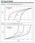
For a 1 volt drop from the 3 volt rail (i.e. VOH = 2 volts) the typical available current is about 7 mA, but may reduce if the chip heats up. However, for this current, the "Low" output voltage (VOL) is only about 0.3 volts. The LTP-305HR Data Sheet indicates that at 7 mA, the voltage drop across each LED is about 1.75 volts, so if we assume one LED connected between a "High" PICaxe Output pin and a "Low" PICaxe Output via a resistor, then the voltage drop across the semiconductors is 1.0 + 1.75 + 0.3 = 3.05 volts. So in this case, no voltage needs to be dropped across the resistor, and zero ohms could/would be used. However, at higher supply voltages, the current might rise dangerously, so the calculation needs to be repeated for the highest supply voltage, to estimate a safe value for the resistor. Then of course, the LEDs would be dimmer at the lower battery voltage.
So far, I've only considered one LED, but the multiplex drives (up to) either 5 or 7 LEDs at a time in parallel, depending whether each set of Anodes (or Cathodes) is being being enabled by a "walking 1" (or a zero). If we consider the display connected directly across a group of (5) "High" PICaxe pins, then the 25 mA Absolute Maximum current permitted to flow into a "Low" PICaxe pin takes priority, i.e. 5 mA through each of 5 LEDs. That's not much less than the "High" pins could deliver anyway, so this looks like quite a "viable" configuration. Rather than try to interpolate values from the 3 and 5 volt graphs, I'll just use the "extreme temperature" lines to "guesstimate" values at (say) a 4 volt supply. Now, the semiconductors would drop 0.5 (VOH Red line for 5mA) + 1.5 (LEDs) + 1.25 (VOL Blue line for 25mA) = 3.25 volts. Therefore at 4 volts, each of the series resistors would be approximately 0.75 / 5 = 150 ohms.
Note that this particular multiplex writes 7 consecutive (5 bit) values to the Anodes' Port, so the average LED current is only 5/7 = 0.71 mA. Therefore the individual LEDs won't be particularly bright, but then they are very small. In principle, the program needs to store 7 bytes for each character/symbol, but the larger M2 chips have 512 bytes of TABLE memory, so storage of a character set shouldn't be a problem. However, for a full (96) ASCII characters (and/or to avoid needing to reconstruct the bitmap tables) it would be possible for a/the PICaxe program to convert each 7x5 array to a 5x7 array in advance, or even "on the fly".
For a brighter display, it's necessary to add 5 pull-up transistors to drive the Anodes (columns) with more current. Now, the pull-down (Cathode rows) drivers limit the usable current, i.e. to a maximum of 25 mA per LED, so the pullup transistors would be rated up to about 175 mA, and the average LED current becomes 25/5 = 5 mA. However, a further restriction in the data sheet is that the total Vss (Earth pin) current must not exceed 85 mA, so we need to halve those currents. At this current the LED voltage drop is approaching 2 volts and the VOL 0.5 volts, so there's about 1.5 volts available across the upper transistor (at 85 mA) plus the series resistor. A conventional (NPN) Emitter Follower might drop 1 volt, leaving about 0.5 volt across each Cathode series resistor, i.e. 0.5 v / 12 mA = 39 ohms. Alternatively, PNP Anode drivers might drop around 0.5 volt, leaving 1 volt across each series resistor, i.e. about 82 ohms.
An advantage of the higher resistance and voltage drop is that the current will vary less when the batteries discharge. Note that the schematic linked in post #5 above uses 330 ohm resistors, so the LED (pulse) currents are never going to be more than a few mA, and the LEDs probably won't be much brighter than the directly driven design in the earlier paragraphs.
Well, that's probably enough for now, but feel free to ask for any clarifications. Actually, I believe I have a "back of envelope" (literally) design concept which meets ALL of your specification in post #13 (i.e. a tiny "backpack" on a LTP-305HR), using only a 14M2 and a few other through-hole components. I'll post this later, if I don't discover any "flaws" or oversights in its operation, after more analysis.
Cheers, Alan.
An efficient hardware design needs a consideration of some "numbers" (from data sheets) and an appreciation of the "asymmetry" of many of the components. Of course a Diode (or LED) is highly asymmetrical; In one direction absolutely no current should flow, whilst in the other direction any current flow should be almost unconstrained - although with a significant (and generally known) forward voltage drop. But also, the display itself is asymmetric, because it has 5 Columns and 7 Rows, which cannot be simply exchanged. Furthermore, the Output Pin drivers inside the PIC(axe) are not symmetrical, the voltage drop across the upper FET (i.e. its resistance) is significantly higher than across the lower FET (at a similar current)..... I would defer to others on the best hardware drive and connection -
The Microchip "base Data Sheet" via this link has some revealing graphs buried in section 31, typically Figures 31-41 to 31-46 in the corresponding 20M2 data sheet. They show the voltage drop across the upper and lower output FETs at various temperatures and at different supply voltages (5v , 3v and 1.8v). It's rarely appreciated how much their resistance increases at the lower rail voltages and at high temperatures. There is no data specifically for 3.7 volts (e.g. a Lithium rechargeable cell) but 3 volts is sometimes considered to be their "discharged" state (particularly by manufacturers trying to maximise their specified capacity). Personally, I normally assume 3.6 volts (also for 3 x discharged NiMH cells) and ideally should take an average between the 3 and 5 volt curves, but for simplicity, here is an example of how one might use only the 3 volt curves:
For a 1 volt drop from the 3 volt rail (i.e. VOH = 2 volts) the typical available current is about 7 mA, but may reduce if the chip heats up. However, for this current, the "Low" output voltage (VOL) is only about 0.3 volts. The LTP-305HR Data Sheet indicates that at 7 mA, the voltage drop across each LED is about 1.75 volts, so if we assume one LED connected between a "High" PICaxe Output pin and a "Low" PICaxe Output via a resistor, then the voltage drop across the semiconductors is 1.0 + 1.75 + 0.3 = 3.05 volts. So in this case, no voltage needs to be dropped across the resistor, and zero ohms could/would be used. However, at higher supply voltages, the current might rise dangerously, so the calculation needs to be repeated for the highest supply voltage, to estimate a safe value for the resistor. Then of course, the LEDs would be dimmer at the lower battery voltage.
So far, I've only considered one LED, but the multiplex drives (up to) either 5 or 7 LEDs at a time in parallel, depending whether each set of Anodes (or Cathodes) is being being enabled by a "walking 1" (or a zero). If we consider the display connected directly across a group of (5) "High" PICaxe pins, then the 25 mA Absolute Maximum current permitted to flow into a "Low" PICaxe pin takes priority, i.e. 5 mA through each of 5 LEDs. That's not much less than the "High" pins could deliver anyway, so this looks like quite a "viable" configuration. Rather than try to interpolate values from the 3 and 5 volt graphs, I'll just use the "extreme temperature" lines to "guesstimate" values at (say) a 4 volt supply. Now, the semiconductors would drop 0.5 (VOH Red line for 5mA) + 1.5 (LEDs) + 1.25 (VOL Blue line for 25mA) = 3.25 volts. Therefore at 4 volts, each of the series resistors would be approximately 0.75 / 5 = 150 ohms.
Note that this particular multiplex writes 7 consecutive (5 bit) values to the Anodes' Port, so the average LED current is only 5/7 = 0.71 mA. Therefore the individual LEDs won't be particularly bright, but then they are very small. In principle, the program needs to store 7 bytes for each character/symbol, but the larger M2 chips have 512 bytes of TABLE memory, so storage of a character set shouldn't be a problem. However, for a full (96) ASCII characters (and/or to avoid needing to reconstruct the bitmap tables) it would be possible for a/the PICaxe program to convert each 7x5 array to a 5x7 array in advance, or even "on the fly".
For a brighter display, it's necessary to add 5 pull-up transistors to drive the Anodes (columns) with more current. Now, the pull-down (Cathode rows) drivers limit the usable current, i.e. to a maximum of 25 mA per LED, so the pullup transistors would be rated up to about 175 mA, and the average LED current becomes 25/5 = 5 mA. However, a further restriction in the data sheet is that the total Vss (Earth pin) current must not exceed 85 mA, so we need to halve those currents.
At this current the LED voltage drop is approaching 2 volts and the VOL 0.5 volts, so there's about 1.5 volts available across the upper transistor (at 85 mA) plus the series resistor. A conventional (NPN) Emitter Follower might drop 1 volt, leaving about 0.5 volt across each Cathode series resistor, i.e. 0.5 v / 12 mA = 39 ohms. Alternatively, PNP Anode drivers might drop around 0.5 volt, leaving 1 volt across each series resistor, i.e. about 82 ohms. An advantage of the higher resistance and voltage drop is that the current will vary less when the batteries discharge. Note that the schematic linked in post #5 above uses 330 ohm resistors, so the LED (pulse) currents are never going to be more than a few mA, and the LEDs probably won't be much brighter than the directly driven design in the earlier paragraphs.
Well, that's probably enough for now, but feel free to ask for any clarifications. Actually, I believe I have a "back of envelope" (literally) design concept which meets ALL of your specification in post #13 (i.e. a tiny "backpack" on a LTP-305HR), using only a 14M2 and a few other through-hole components. I'll post this later, if I don't discover any "flaws" or oversights in its operation, after more analysis.
Cheers, Alan.
If you connected anodes directly to pins rather than using transistors each pin can source or sink ~20mA, so each sink (C.x low) would be sinking 7 sources with a column fully lit (B.x all high), which would mean 3mA per source, so 1K8 per B.x line ought to have it working.So simple when you know what you're doing
That might not be very bright but it will allow you to prototype and develop the software while you plan how to do the display side of things. And might actually prove to be be bright enough.
You would need to switch the "HIGH/LOW col" lines because the transistor inversion has been removed.
Allen - I took the time to read your post several times. There are a lot of details I had to understand that I normally gloss over. Yes indeed, the devil is in the details. All my projects up to this point didn't approach any limits of picaxe and I had a LOT of room for circuits that were "sloppy" but still worked well. I think this project needs that attention to detail to work the way it should. By all means PLEASE post your circuit when it passes your muster. Any information is always helpful.Hi,
An efficient hardware design needs a consideration of some "numbers" (from data sheets) and an appreciation of the "asymmetry" of many of the components. Of course a Diode (or LED) is highly asymmetrical; In one direction absolutely no current should flow, whilst in the other direction any current flow should be almost unconstrained - although with a significant (and generally known) forward voltage drop. But also, the display itself is asymmetric, because it has 5 Columns and 7 Rows, which cannot be simply exchanged. Furthermore, the Output Pin drivers inside the PIC(axe) are not symmetrical, the voltage drop across the upper FET (i.e. its resistance) is significantly higher than across the lower FET (at a similar current).
The Microchip "base Data Sheet" via this link has some revealing graphs buried in section 31, typically Figures 31-41 to 31-46 in the corresponding 20M2 data sheet. They show the voltage drop across the upper and lower output FETs at various temperatures and at different supply voltages (5v , 3v and 1.8v). It's rarely appreciated how much their resistance increases at the lower rail voltages and at high temperatures. There is no data specifically for 3.7 volts (e.g. a Lithium rechargeable cell) but 3 volts is sometimes considered to be their "discharged" state (particularly by manufacturers trying to maximise their specified capacity). Personally, I normally assume 3.6 volts (also for 3 x discharged NiMH cells) and ideally should take an average between the 3 and 5 volt curves, but for simplicity, here is an example of how one might use only the 3 volt curves:
View attachment 25294
For a 1 volt drop from the 3 volt rail (i.e. VOH = 2 volts) the typical available current is about 7 mA, but may reduce if the chip heats up. However, for this current, the "Low" output voltage (VOL) is only about 0.3 volts. The LTP-305HR Data Sheet indicates that at 7 mA, the voltage drop across each LED is about 1.75 volts, so if we assume one LED connected between a "High" PICaxe Output pin and a "Low" PICaxe Output via a resistor, then the voltage drop across the semiconductors is 1.0 + 1.75 + 0.3 = 3.05 volts. So in this case, no voltage needs to be dropped across the resistor, and zero ohms could/would be used. However, at higher supply voltages, the current might rise dangerously, so the calculation needs to be repeated for the highest supply voltage, to estimate a safe value for the resistor. Then of course, the LEDs would be dimmer at the lower battery voltage.
So far, I've only considered one LED, but the multiplex drives (up to) either 5 or 7 LEDs at a time in parallel, depending whether each set of Anodes (or Cathodes) is being being enabled by a "walking 1" (or a zero). If we consider the display connected directly across a group of (5) "High" PICaxe pins, then the 25 mA Absolute Maximum current permitted to flow into a "Low" PICaxe pin takes priority, i.e. 5 mA through each of 5 LEDs. That's not much less than the "High" pins could deliver anyway, so this looks like quite a "viable" configuration. Rather than try to interpolate values from the 3 and 5 volt graphs, I'll just use the "extreme temperature" lines to "guesstimate" values at (say) a 4 volt supply. Now, the semiconductors would drop 0.5 (VOH Red line for 5mA) + 1.5 (LEDs) + 1.25 (VOL Blue line for 25mA) = 3.25 volts. Therefore at 4 volts, each of the series resistors would be approximately 0.75 / 5 = 150 ohms.
Note that this particular multiplex writes 7 consecutive (5 bit) values to the Anodes' Port, so the average LED current is only 5/7 = 0.71 mA. Therefore the individual LEDs won't be particularly bright, but then they are very small. In principle, the program needs to store 7 bytes for each character/symbol, but the larger M2 chips have 512 bytes of TABLE memory, so storage of a character set shouldn't be a problem. However, for a full (96) ASCII characters (and/or to avoid needing to reconstruct the bitmap tables) it would be possible for a/the PICaxe program to convert each 7x5 array to a 5x7 array in advance, or even "on the fly".
For a brighter display, it's necessary to add 5 pull-up transistors to drive the Anodes (columns) with more current. Now, the pull-down (Cathode rows) drivers limit the usable current, i.e. to a maximum of 25 mA per LED, so the pullup transistors would be rated up to about 175 mA, and the average LED current becomes 25/5 = 5 mA. However, a further restriction in the data sheet is that the total Vss (Earth pin) current must not exceed 85 mA, so we need to halve those currents.
An advantage of the higher resistance and voltage drop is that the current will vary less when the batteries discharge. Note that the schematic linked in post #5 above uses 330 ohm resistors, so the LED (pulse) currents are never going to be more than a few mA, and the LEDs probably won't be much brighter than the directly driven design in the earlier paragraphs.
Well, that's probably enough for now, but feel free to ask for any clarifications. Actually, I believe I have a "back of envelope" (literally) design concept which meets ALL of your specification in post #13 (i.e. a tiny "backpack" on a LTP-305HR), using only a 14M2 and a few other through-hole components. I'll post this later, if I don't discover any "flaws" or oversights in its operation, after more analysis.
Cheers, Alan.
If you connected anodes directly to pins rather than using transistors each pin can source or sink ~20mA, so each sink (C.x low) would be sinking 7 sources with a column fully lit (B.x all high), which would mean 3mA per source, so 1K8 per B.x line ought to have it working.
That might not be very bright but it will allow you to prototype and develop the software while you plan how to do the display side of things. And might actually prove to be be bright enough.
You would need to switch the "HIGH/LOW col" lines because the transistor inversion has been removed.
That thought occurred to as well. I'm not sure, but I believe the transistors are there to provide a bit of a constant current to maintain somewhat stable brightness? There is every possibility that I could be 100% wrong about this however. That's part of the fun - experimenting. I will definitely try your suggestion and see what the results are.
Hi,
However, I don't believe that a constant current is the intention (or capability) of the transistors in the circuit linked in post #5. A fundamental feature of the "multiplexed" drive is that a group of 5 (or 7) LEDs is driven by a single transistor at one end, but by 5 (or 7) separate transistors at their other end. This means that the one transistor must have a current capability 5 or 7 times larger than the others, so it is traditional to use a more powerful transistor, or even an additional amplifier stage, in this position. Since the specification of the transistors within the PIC(axe) is not within our control (or choice), then the "obvious" arrangement is to add external transistors in the "higher current" position. But IMHO, those in the linked post may be achieving rather little in practice, because the current (probably a few mA) is limited mainly by the choice of the 330 ohm resistors in association with the 1 volt drop across the emitter follower driver configuration.
For our case here, the design is complicated because the PIC's upper and lower output transistors (FETs) have different current capabilities, as described above in #23. Thus there is a whole spectrum of possible configurations giving gradually higher current (i.e. brightness) capabilities. To summarise my above post, we probably should assume a supply rail of 4 volts (for a single lithium rechargeable cell), so take average data from the 3 and 5 volt graphs. In practice, it appears that the curves for 3 volts at -40 degrees C and 5 volts at +125 degrees C are quite similar, so we can use either of those as a reasonable indicator for operation at 4 volts with a more typical temperature. Note that it's not the "VOH" which we normally need to consider, but the voltage drop (Vdd - VOH) down from the supply rail (i.e. the point where the curves meet, at zero current). From those graphs, the Voltage drops which might come in useful are (for an M2 PICaxe) :
Upper transistor at 3.5 mA = 0.3 volt
Upper transistor at 9 mA = 1.0 volt
Lower transistor at 2 mA = 0.1 volt
Lower transistor at 12 mA = 0.4 volt
Lower transistor at 24 mA (max) = 1.1 volts
External transistor at 85 mA = 0.5 volt (typical if saturated, but depends on base current, etc.)
LED (forward) around 1 mA = 1.75 volts
LED (forward) at 12 mA = 1.9 volts
Starting with the simplest (but also lowest brightness) directly-driven multiplex, we would generate a "walking 1" from the pins of a PICaxe port to the (5) LED Anode Columns. Preferably the pins/columns should be driven in the same sequence (e.g. left to right), but they could be "re-arranged" in the program software if necessary (e.g. by using a LOOKUP or READ{TABLE} method). Then, the pins of another port are arranged to pull the LED Cathode/Row pins LOW for any LED which is required to be illuminated. Again it is preferable to "map" the pins/rows in sequence, but not absolutely essential.
The maximum available current from the HIGH pin is about 9 mA (@Vdd = 4v), which has to be shared by up to 7 LEDs, so the current in each LED may be about only 9 / 7 = 1.3 mA. Then, the duration of the "1" is at most 1/5 of the total cycle time, so the average LED current is 0.25 mA, even assuming that the program can switch very rapidly from one "pattern" to the next:
Thus the Anode/Column and Cathode/Row pin patterns need to be updated by "consecutive" program instructions, but even then, there may be an "incorrect" pattern of LEDs illuminated during the intervening period. Therefore, it's usually better/necessary to switch OFF one of the Ports, change the bits on the other Port and then re-activate the first port with its new bit-pattern. The reason for doing this is that switching OFF a lit LED for a brief period will make no apparent difference to its brightness, but switching ON a LED for even a very brief period, when it should be be OFF, may make it noticeably glow a little (at least in a low ambient light level).
In this example, the voltage drop across the semiconductors (i.e. the PICaxe and LED display) is about 1.0 + 1.75 + 0.1 = 2.85 volts, leaving about 4.0 - 2.85 = 1.15 volts across each resistor. The (7) resistors are required to balance or limit the current in each LED, so are connected in series with each Cathode/Row display pin, with a value of V / I = 1.15 / 1.3 = 880 ohms, say 820 or 1k ohms.
The first improvement is to use instead a "walking 0" across the Cathode/Row pins; This can sink up to 24 mA, shared across the (5) columns, so 4.8 mA for each LED. That has a maximum duty cycle of only 1/7, but the resulting average of 24 / 35 = 0.68 mA is almost 2.5 times the previous arrangement. Ideally, the port update rate should be shorter at about 5 / 7 = 71% of the previous period, but the refresh/update rate is unlikely to be a serious problem in practice. In this configuration, the (5) resistors must be in series with the Anode/Column pins; the voltage across them about 4.0 - (0.3 + 1.75 + 1.1) = 0.85 volts and their resistance 0.85 / 4.8 = 180 , or 220 ohms.
The next "improvement" could be to add NPN transistors to sink current from the (7) Cathode/Row pins, which would allow each Column driver to run its LED at 9 mA (i.e. a total up to 45 mA), for another current increase of about twice (to 45/35 = 1.3 mA per LED). However, that needs 7 transistors (and resistors) to be added, so it's better to use transistors to drive the (5) Anode/Columns at a still higher current. Here, the limiting current is the 85 mA of the PICaxe package Ground pin, giving an LED pulse current of 85 / 7 = 12 mA and an average of 12 / 5 = 2.4 mA, almost doubling the LED current yet again. The (7) current balancing/limiting resistors would be in series with the Cathode/Row pins, but their value is a little dependent on the (NPN or PNP) driver configuration:
The emitter ("follower") of a NPN transistor will be about 1 volt below the supply rail, made up of its Vbe (~700mV) and the PICaxe output drop of about 300 mV (for a base current of perhaps 1 mA); there is no need for a resistor between the PICaxe pin and the NPN's base. Thus the voltage across the resistor(s) will be about 4.0 - (1.0 + 1.75 + 0.4) = 0.85 volts and their value about 0.85 / 12 = 70 ohms, say 68 or 56. With a 4 volt supply, this is probably the "optimum" configuration, but if the rail is likely to fall to 3.5 volts or below, then it might be better to use a PNP transistor, driven by a base current of several mA through a resistor from the (now inverted) active low outputs of the PICaxe. The lower "saturation voltage" of the PNP can give more "headroom" when the supply voltage falls, or there is some scope for restricting the base current, to give a partial "constant current" drive capability.
Finally, we could use driver transistors for both the Rows and Columns, to run the display LEDs up to their "maximum" rating (and brightness), but note that the data sheet specifies the pulse current at 10%, 1 kHz, whilst a PICaxe is unlikely to give an update frequency faster than about 50 - 60 Hz.
Well again, that must be more than enough for now, but I may follow with a separate post for my "14M2" concept, in due course.
Cheers, Alan.
You're correct that some of the dedicated "LED Display Driver ICs" do have a "constant-current" output stage (perhaps controlled by a "brightness" register), intended to give a "Plug and Play" or "Fit and Forget" type of capability. A "problem" with LEDs is that they have primarily a constant (forward) voltage drop characteristic, so a small change in the applied voltage can cause a very large change in the current that flows (assuming it's available from the supply). Thus, they are usually connected in series with a resistor, but the resistor doesn't contribute to any light output, it just "wastes" energy (as heat). Therefore, the temptation is to make the resistance value (and hence voltage drop) as low as possible. But if most of the voltage drops in the circuit are "fixed" (e.g. the LED/diode/transistor forward/saturation drops), then small changes/errors in the supply rail can produce very large brightness variations...... I believe the transistors are there to provide a bit of a constant current to maintain somewhat stable brightness?
However, I don't believe that a constant current is the intention (or capability) of the transistors in the circuit linked in post #5. A fundamental feature of the "multiplexed" drive is that a group of 5 (or 7) LEDs is driven by a single transistor at one end, but by 5 (or 7) separate transistors at their other end. This means that the one transistor must have a current capability 5 or 7 times larger than the others, so it is traditional to use a more powerful transistor, or even an additional amplifier stage, in this position. Since the specification of the transistors within the PIC(axe) is not within our control (or choice), then the "obvious" arrangement is to add external transistors in the "higher current" position. But IMHO, those in the linked post may be achieving rather little in practice, because the current (probably a few mA) is limited mainly by the choice of the 330 ohm resistors in association with the 1 volt drop across the emitter follower driver configuration.
For our case here, the design is complicated because the PIC's upper and lower output transistors (FETs) have different current capabilities, as described above in #23. Thus there is a whole spectrum of possible configurations giving gradually higher current (i.e. brightness) capabilities. To summarise my above post, we probably should assume a supply rail of 4 volts (for a single lithium rechargeable cell), so take average data from the 3 and 5 volt graphs. In practice, it appears that the curves for 3 volts at -40 degrees C and 5 volts at +125 degrees C are quite similar, so we can use either of those as a reasonable indicator for operation at 4 volts with a more typical temperature. Note that it's not the "VOH" which we normally need to consider, but the voltage drop (Vdd - VOH) down from the supply rail (i.e. the point where the curves meet, at zero current). From those graphs, the Voltage drops which might come in useful are (for an M2 PICaxe) :
Upper transistor at 3.5 mA = 0.3 volt
Upper transistor at 9 mA = 1.0 volt
Lower transistor at 2 mA = 0.1 volt
Lower transistor at 12 mA = 0.4 volt
Lower transistor at 24 mA (max) = 1.1 volts
External transistor at 85 mA = 0.5 volt (typical if saturated, but depends on base current, etc.)
LED (forward) around 1 mA = 1.75 volts
LED (forward) at 12 mA = 1.9 volts
Starting with the simplest (but also lowest brightness) directly-driven multiplex, we would generate a "walking 1" from the pins of a PICaxe port to the (5) LED Anode Columns. Preferably the pins/columns should be driven in the same sequence (e.g. left to right), but they could be "re-arranged" in the program software if necessary (e.g. by using a LOOKUP or READ{TABLE} method). Then, the pins of another port are arranged to pull the LED Cathode/Row pins LOW for any LED which is required to be illuminated. Again it is preferable to "map" the pins/rows in sequence, but not absolutely essential.
The maximum available current from the HIGH pin is about 9 mA (@Vdd = 4v), which has to be shared by up to 7 LEDs, so the current in each LED may be about only 9 / 7 = 1.3 mA. Then, the duration of the "1" is at most 1/5 of the total cycle time, so the average LED current is 0.25 mA, even assuming that the program can switch very rapidly from one "pattern" to the next:
Thus the Anode/Column and Cathode/Row pin patterns need to be updated by "consecutive" program instructions, but even then, there may be an "incorrect" pattern of LEDs illuminated during the intervening period. Therefore, it's usually better/necessary to switch OFF one of the Ports, change the bits on the other Port and then re-activate the first port with its new bit-pattern. The reason for doing this is that switching OFF a lit LED for a brief period will make no apparent difference to its brightness, but switching ON a LED for even a very brief period, when it should be be OFF, may make it noticeably glow a little (at least in a low ambient light level).
In this example, the voltage drop across the semiconductors (i.e. the PICaxe and LED display) is about 1.0 + 1.75 + 0.1 = 2.85 volts, leaving about 4.0 - 2.85 = 1.15 volts across each resistor. The (7) resistors are required to balance or limit the current in each LED, so are connected in series with each Cathode/Row display pin, with a value of V / I = 1.15 / 1.3 = 880 ohms, say 820 or 1k ohms.
The first improvement is to use instead a "walking 0" across the Cathode/Row pins; This can sink up to 24 mA, shared across the (5) columns, so 4.8 mA for each LED. That has a maximum duty cycle of only 1/7, but the resulting average of 24 / 35 = 0.68 mA is almost 2.5 times the previous arrangement. Ideally, the port update rate should be shorter at about 5 / 7 = 71% of the previous period, but the refresh/update rate is unlikely to be a serious problem in practice. In this configuration, the (5) resistors must be in series with the Anode/Column pins; the voltage across them about 4.0 - (0.3 + 1.75 + 1.1) = 0.85 volts and their resistance 0.85 / 4.8 = 180 , or 220 ohms.
The next "improvement" could be to add NPN transistors to sink current from the (7) Cathode/Row pins, which would allow each Column driver to run its LED at 9 mA (i.e. a total up to 45 mA), for another current increase of about twice (to 45/35 = 1.3 mA per LED). However, that needs 7 transistors (and resistors) to be added, so it's better to use transistors to drive the (5) Anode/Columns at a still higher current. Here, the limiting current is the 85 mA of the PICaxe package Ground pin, giving an LED pulse current of 85 / 7 = 12 mA and an average of 12 / 5 = 2.4 mA, almost doubling the LED current yet again. The (7) current balancing/limiting resistors would be in series with the Cathode/Row pins, but their value is a little dependent on the (NPN or PNP) driver configuration:
The emitter ("follower") of a NPN transistor will be about 1 volt below the supply rail, made up of its Vbe (~700mV) and the PICaxe output drop of about 300 mV (for a base current of perhaps 1 mA); there is no need for a resistor between the PICaxe pin and the NPN's base. Thus the voltage across the resistor(s) will be about 4.0 - (1.0 + 1.75 + 0.4) = 0.85 volts and their value about 0.85 / 12 = 70 ohms, say 68 or 56. With a 4 volt supply, this is probably the "optimum" configuration, but if the rail is likely to fall to 3.5 volts or below, then it might be better to use a PNP transistor, driven by a base current of several mA through a resistor from the (now inverted) active low outputs of the PICaxe. The lower "saturation voltage" of the PNP can give more "headroom" when the supply voltage falls, or there is some scope for restricting the base current, to give a partial "constant current" drive capability.
Finally, we could use driver transistors for both the Rows and Columns, to run the display LEDs up to their "maximum" rating (and brightness), but note that the data sheet specifies the pulse current at 10%, 1 kHz, whilst a PICaxe is unlikely to give an update frequency faster than about 50 - 60 Hz.
Well again, that must be more than enough for now, but I may follow with a separate post for my "14M2" concept, in due course.
Cheers, Alan.
Last edited:
Technoman
Senior Member
@AllyCat : thank you for your answer.
After some search, this website gave me a better understanding of the clock configuration.
https://www.mikroe.com/ebooks/pic-microcontrollers-programming-in-basic/clock-oscillator
Surprisingly, I was not able to locate any block diagram for the 16F1829 on the Microchip's website.
After some search, this website gave me a better understanding of the clock configuration.
https://www.mikroe.com/ebooks/pic-microcontrollers-programming-in-basic/clock-oscillator
Surprisingly, I was not able to locate any block diagram for the 16F1829 on the Microchip's website.
Hi,
Cheers, Alan.
It's a complex chip so there probably isn't any single "bock diagram", but the 436 page PIC16(L)F1825/9 Data Sheet has "Top Level" diagrams in Figure1-1 (Page 10) and Figure 2-1, etc.. Then more block details in the individual "Module" sections, for example Figure 5-1 for the Clock Block Diagram, etc.. Not as "colourful" as your link, but I think the basic information should all be there.Surprisingly, I was not able to locate any block diagram for the 16F1829 on the Microchip's website.
Cheers, Alan.
Hi,
Generally, I strive to absolutely minimise the number of external components in any circuit design, particularly with Microchip devices that have such an impressive number of additional on-chip functions (Gates, Op-Amps, etc.). The additional price of a package with more pins is relatively small, whilst the "cost" of external components should include the design, assembly, testing, circuit board area and inventory, etc.. The 7x5 Matrix/display in this thread is so tiny that additional (driver) transistors shouldn't be necessary (unless used outdoors?), but it requires 12 pin connections so the "obvious" PICaxe to choose is an 18 or 20M2. However, the following requirement/specification from post #13 might make this a "special case" :
The feature which allows a 14M2 to drive all 12 display pins is that only one pin in either the Row or Column group needs to be selected at any instant in time (i.e. with a "walking 0" or "1" logic level moving across the port). This could be implemented by a hardware Shift Register (a common method with Multiplexed/Matrix displays), but adding another IC package is not sensible in this application (particularly as most standard "logic" families have a lower current-drive capability than the PIC{axe} ports). The characteristic employed here is that most PICaxe pins have a "Tri-State" output capability, i.e. "Low", "High" and "Floating" (implemented by an INPUT or DIRS command/variable). Thus, each of 3 pins (C.0 , C.1 and C.2 chosen here) can directly drive one of three Display Row pins "Low", OR output a "High" to activate one of three external transistors, each pulling another associated display pin "Low". Therefore, only 3 PICaxe pins are required to control 6 Display pins, with a 4th pin driving the 7th Display Row in a normal manner. This 4th pin might be C.3 (using its internal "Weak Pullup resistor" and another external transistor) or C.4 directly. However, C.4 is the only free, full I/O pin now available for any "User" application, so here I have allocated the serial output (B.0) to drive the final Row pin.
Floating (i.e. Tri-Stating) the PICaxe pins can work very well, but we must not overlook that there are 5 LEDs (Cathodes) inside the display package, which are also connected to each Row Pin. Therefore, we must consider any currents which might flow through this array and interfere with the operation of the external transistor(s): Thus, always one of the pull-down Row-driver transistors should be active (at least whenever a Column pin is being pulled High) to limit the highest voltage on the Anodes. Then a "worst case" is when all 5 groups of LEDs are pulled High by the Column Drivers, so typically 20 mA would flow through the (PICaxe) active Row-driver pin. This could pull the pin up to 0.75 volt above Ground, then the forward drop of about 1.75 volts across any activated LED, would take the Common Anode matrix lines/pins up to about 2.5 volts above ground:
Thus, the other LEDs in the array may "leak" a current (of many uA) to all the other Cathodes, through a forward voltage drop of say 1.5 volts, such that up to 1 volt may appear on the Row pin(s) that are intended to be "floating". Normally, the base of a bipolar transistor needs to be held below about 400 mV to ensure that it is completely OFF, so a potential divider of 4k7 + 2k2 is used to reduce the 1v input to around 2k2 / 6k9 = 320 mV. At other times when the PICaxe output is pulled HIGH, the 4k7 passes about 400 uA into the base (with a further ~270 uA through the 2k2 drain) to switch ON the transistor. This base current is chosen unusually low: Data Sheets typically specify the "Collector Saturation voltage" at 10 times the base current (i.e. 20 mA / 10 = 2 mA, but "hard" saturation is not required here, for a Vce ON around 0.75v (i.e. equivalent to the level achieved by the PICaxe). Therefore a value of "collector current / 50" should be satisfactory for a device such as the BC548, which has a current capability up to 100 mA and a gain that peaks around 20 mA.
Another complication is that the 4k7 + 2k2 resistor chain itself can pull about 1 / 6.9k = 150 uA through any LED that has its Anode pulled High, which may cause it to glow dimly (but clearly noticeable in low ambient light levels). Two alternative solutions have been considered:
The first method is to Activate the PICaxe's "Weak Pullup" resistors when the associated PICaxe pins are configured as Input or Floating. These Pullups are typically 30k ohms or 130 uA output (at 4 volts; max 200 uA), which should bias the Cathode/Row pins high enough that current won't flow significantly through the (unselected) LEDs. It was primarily the WPU resistor values that determined the choice of the 4k7 + 2k2 values to achieve this, whilst not turning the transistor ON.
The alternative solution is to use a FET driver such as the popular 2N7000, which should easily saturate at a Gate voltage above ~3.5v and be OFF below 1 volt (but neither value is absolutely "guaranteed" by its data sheet). In this case (shown in one of the Row driver positions below) the input series resistance is zero (to maximise the Gate voltage), whilst a light pull-down is still required to overcome the floating input. But this resistor should be much higher at 100k or even 1M ohm (with the WPU NOT activated) to avoid illuminating the display LED (or switching ON the FET). In addition to saving one resistor per stage, the FET has an advantage that both its Gate and Drain can be wired directly to two (Cathode) pins of the display, which may simplify the overall circuit board layout.
Here is a suggested schematic diagram, it's not tested (and cannot be, because I don't have that particular Display) but I'm moderately confident that it should work. However, caution is always needed with a Multiplexed display, because currents or voltages can take "unexpected" paths through the matrix and "spoil" the display. Note that for the serial input pin (C.5), only the 100k pulldown resistor is essential; the 22k and programming adapter may be connected externally as/when required.
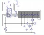
Personally, if I were constructing (one of) such a module, I still prefer to use through-hole components, but the pins of the two identical footprint packages must compete for "hole" locations on both sides of a single circuit board. Therefore, I would employ two similar "Pseudo PCB" prototyping boards (Vero, Strip or Pad Boards, etc.), one each for the Display and PICaxe, the same size as the DIL package (i.e. 4 x 7 holes) forming the "bread" of a sandwich, with the discrete components (particularly resistors) mounted vertically as the "meat" in the sandwich. The majority of the discrete components would occupy the two rows of holes between the DIL package pins, but some (transistors in particular) could be soldered directly onto the back of the DIL package/socket pins to which they need to connect. However, the pinout of the LTP-305 display package is so "horrible" (with no logical external pattern of pin functions) that it may be necessary to adopt any convenient pin sequence to link each Port to its respective Anode or Cathode pins, and then "unscramble" the bits with a simple Lookup (Table) in the Program.
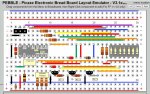
Here is a "Pebble" layout which IMHO can give a good compromise between a Schematic and Layout design presentation (but it has no Simulation, Analysis or "Sanity" Checking capabilities). The Port.Pin to Column/Row pin sequences should be shown correctly, but it might not be possible to achieve this in a "final" (compact) circuit board design. In principle, Pebble can be used also for simple Pseudo-PCB layouts, but probably not for my "three-dimensional" (multi-layer) construction suggested above.
To summarise the overall functionality; the three external transistors are NOT employed to increase the LED's drive current (brightness) but only to act as "gates", adding (3) pin drivers that are not available in the smaller, 14M2 package. The (7) Cathode/Row pins are driven in sequence (i.e. by a "walking 0") with the (5) Anode/Column pins driven in parallel by the appropriate bit-pattern for each Row. The 14M2 doesn't even have a port as wide as 7 bits, so the driver code may be a little "untidy" regardless of how the matrix is driven. Finally, it's worth noting that most PICaxe Output pins can have four states: "Low", "High", "Floating" and "Weak Pullup" (all used above), although it's difficult to devise a simple Hardware configuration to differentiate between all four states.
Cheers, Alan.
Generally, I strive to absolutely minimise the number of external components in any circuit design, particularly with Microchip devices that have such an impressive number of additional on-chip functions (Gates, Op-Amps, etc.). The additional price of a package with more pins is relatively small, whilst the "cost" of external components should include the design, assembly, testing, circuit board area and inventory, etc.. The 7x5 Matrix/display in this thread is so tiny that additional (driver) transistors shouldn't be necessary (unless used outdoors?), but it requires 12 pin connections so the "obvious" PICaxe to choose is an 18 or 20M2. However, the following requirement/specification from post #13 might make this a "special case" :
Normally, a backpack or "daughter board" would be expected to be smaller than (and/or to not overhang the sides of) the main "mother" board or module: Particularly, for a display which might be required to be "End (and/or Side) -Stackable", or to be mounted from the front though a panel cutout. But here, the display is a very small 14-pin DIL (Dual-In-Line) package, obviously shorter than an 18/20 pin DIP PICaxe, and surprisingly, also narrower than the 18/20 pin SMD (SSOP) packages (because the SMD "pins" extend horizontally, rather than bending through 90 degrees into the circuit board). Therefore, the PICaxe 14M2 is worthy of consideration; the DIP is obviously no larger than the Display, and also the SMD (SSOP) version is narrow enough to fit between the pins of the Display package.I only need to drive one small 5 x 7 matrix, .... I want to make this piggy back onto the ltp-305 so I may need to go surface mount as well.
The feature which allows a 14M2 to drive all 12 display pins is that only one pin in either the Row or Column group needs to be selected at any instant in time (i.e. with a "walking 0" or "1" logic level moving across the port). This could be implemented by a hardware Shift Register (a common method with Multiplexed/Matrix displays), but adding another IC package is not sensible in this application (particularly as most standard "logic" families have a lower current-drive capability than the PIC{axe} ports). The characteristic employed here is that most PICaxe pins have a "Tri-State" output capability, i.e. "Low", "High" and "Floating" (implemented by an INPUT or DIRS command/variable). Thus, each of 3 pins (C.0 , C.1 and C.2 chosen here) can directly drive one of three Display Row pins "Low", OR output a "High" to activate one of three external transistors, each pulling another associated display pin "Low". Therefore, only 3 PICaxe pins are required to control 6 Display pins, with a 4th pin driving the 7th Display Row in a normal manner. This 4th pin might be C.3 (using its internal "Weak Pullup resistor" and another external transistor) or C.4 directly. However, C.4 is the only free, full I/O pin now available for any "User" application, so here I have allocated the serial output (B.0) to drive the final Row pin.
Floating (i.e. Tri-Stating) the PICaxe pins can work very well, but we must not overlook that there are 5 LEDs (Cathodes) inside the display package, which are also connected to each Row Pin. Therefore, we must consider any currents which might flow through this array and interfere with the operation of the external transistor(s): Thus, always one of the pull-down Row-driver transistors should be active (at least whenever a Column pin is being pulled High) to limit the highest voltage on the Anodes. Then a "worst case" is when all 5 groups of LEDs are pulled High by the Column Drivers, so typically 20 mA would flow through the (PICaxe) active Row-driver pin. This could pull the pin up to 0.75 volt above Ground, then the forward drop of about 1.75 volts across any activated LED, would take the Common Anode matrix lines/pins up to about 2.5 volts above ground:
Thus, the other LEDs in the array may "leak" a current (of many uA) to all the other Cathodes, through a forward voltage drop of say 1.5 volts, such that up to 1 volt may appear on the Row pin(s) that are intended to be "floating". Normally, the base of a bipolar transistor needs to be held below about 400 mV to ensure that it is completely OFF, so a potential divider of 4k7 + 2k2 is used to reduce the 1v input to around 2k2 / 6k9 = 320 mV. At other times when the PICaxe output is pulled HIGH, the 4k7 passes about 400 uA into the base (with a further ~270 uA through the 2k2 drain) to switch ON the transistor. This base current is chosen unusually low: Data Sheets typically specify the "Collector Saturation voltage" at 10 times the base current (i.e. 20 mA / 10 = 2 mA, but "hard" saturation is not required here, for a Vce ON around 0.75v (i.e. equivalent to the level achieved by the PICaxe). Therefore a value of "collector current / 50" should be satisfactory for a device such as the BC548, which has a current capability up to 100 mA and a gain that peaks around 20 mA.
Another complication is that the 4k7 + 2k2 resistor chain itself can pull about 1 / 6.9k = 150 uA through any LED that has its Anode pulled High, which may cause it to glow dimly (but clearly noticeable in low ambient light levels). Two alternative solutions have been considered:
The first method is to Activate the PICaxe's "Weak Pullup" resistors when the associated PICaxe pins are configured as Input or Floating. These Pullups are typically 30k ohms or 130 uA output (at 4 volts; max 200 uA), which should bias the Cathode/Row pins high enough that current won't flow significantly through the (unselected) LEDs. It was primarily the WPU resistor values that determined the choice of the 4k7 + 2k2 values to achieve this, whilst not turning the transistor ON.
The alternative solution is to use a FET driver such as the popular 2N7000, which should easily saturate at a Gate voltage above ~3.5v and be OFF below 1 volt (but neither value is absolutely "guaranteed" by its data sheet). In this case (shown in one of the Row driver positions below) the input series resistance is zero (to maximise the Gate voltage), whilst a light pull-down is still required to overcome the floating input. But this resistor should be much higher at 100k or even 1M ohm (with the WPU NOT activated) to avoid illuminating the display LED (or switching ON the FET). In addition to saving one resistor per stage, the FET has an advantage that both its Gate and Drain can be wired directly to two (Cathode) pins of the display, which may simplify the overall circuit board layout.
Here is a suggested schematic diagram, it's not tested (and cannot be, because I don't have that particular Display) but I'm moderately confident that it should work. However, caution is always needed with a Multiplexed display, because currents or voltages can take "unexpected" paths through the matrix and "spoil" the display. Note that for the serial input pin (C.5), only the 100k pulldown resistor is essential; the 22k and programming adapter may be connected externally as/when required.
Personally, if I were constructing (one of) such a module, I still prefer to use through-hole components, but the pins of the two identical footprint packages must compete for "hole" locations on both sides of a single circuit board. Therefore, I would employ two similar "Pseudo PCB" prototyping boards (Vero, Strip or Pad Boards, etc.), one each for the Display and PICaxe, the same size as the DIL package (i.e. 4 x 7 holes) forming the "bread" of a sandwich, with the discrete components (particularly resistors) mounted vertically as the "meat" in the sandwich. The majority of the discrete components would occupy the two rows of holes between the DIL package pins, but some (transistors in particular) could be soldered directly onto the back of the DIL package/socket pins to which they need to connect. However, the pinout of the LTP-305 display package is so "horrible" (with no logical external pattern of pin functions) that it may be necessary to adopt any convenient pin sequence to link each Port to its respective Anode or Cathode pins, and then "unscramble" the bits with a simple Lookup (Table) in the Program.
Here is a "Pebble" layout which IMHO can give a good compromise between a Schematic and Layout design presentation (but it has no Simulation, Analysis or "Sanity" Checking capabilities). The Port.Pin to Column/Row pin sequences should be shown correctly, but it might not be possible to achieve this in a "final" (compact) circuit board design. In principle, Pebble can be used also for simple Pseudo-PCB layouts, but probably not for my "three-dimensional" (multi-layer) construction suggested above.
To summarise the overall functionality; the three external transistors are NOT employed to increase the LED's drive current (brightness) but only to act as "gates", adding (3) pin drivers that are not available in the smaller, 14M2 package. The (7) Cathode/Row pins are driven in sequence (i.e. by a "walking 0") with the (5) Anode/Column pins driven in parallel by the appropriate bit-pattern for each Row. The 14M2 doesn't even have a port as wide as 7 bits, so the driver code may be a little "untidy" regardless of how the matrix is driven. Finally, it's worth noting that most PICaxe Output pins can have four states: "Low", "High", "Floating" and "Weak Pullup" (all used above), although it's difficult to devise a simple Hardware configuration to differentiate between all four states.
Cheers, Alan.
Last edited:
Hello Allan - Thank you very much for taking the time to work this out. I have read through your explanation a few times and feel I have a good handle on what's going on. You have hit on many details I missed in my original design/thoughts. My design never would have worked. For instance, I naturally "assumed" the surface mount package would be more than small enough to fit behind the display! I have all the items I need to start the build up. I managed to break my ankle mountain biking a few weeks ago and am in quite a bit of pain right now. Once I can hobble around a bit, I will resume this project and update you.