Driving MOSFETs

Haku

Senior Member
I have a Picaxe being powered from a 78L05 which in turn is being powered from a 10v source.

I want the Picaxe to send 10v (in pulses) to an array of 12 parallel IRFZ46N MOSFETs (datasheet).

The programming is sorted but I have to admit defeat on figuring out how I can trigger the MOSFETs with a transistor.

Can anyone help?
 

premelec

Senior Member
Bipolar pull down

You can put a resistor to V10+ on each gate and then 1K from PICAXE pin to the base of an NPN transistor and emitter goes to V- and collector to the gate - this should work unless you have very high speed switching needs - the gate has large capacitance and so must be driven up and down for high speed - the single transistor circuit I've suggested will pull down fast but turn on slower with the RC of the gate cap and pullup resistor....
 

Dippy

Moderator
Haku, you've been a Forumite for quite a time; so, can you post a basic schematic of how you want this configured, just something rough. And give more details.

I find "to send 10v (in pulses) to an array of 12 parallel IRFZ46N MOSFETs" to be very ambiguous.
Do you mean 10V to the Gate? Or as a 'supply' to the whole array?
Is this 'array' a pile of paralleled MOSFETs or does each MOSFET switch separately?
Why did you choose that MOSFET?

"how I can trigger the MOSFETs with a transistor"
- what kind of transistor?

Is it going to be PWM'd? What frequency?

The precise application requirement will determine the design.

As said by MPep, MOSFET driving has been discussed many, many times and a 20 minute search by you will probably reveal 90% of the answer.
 

Haku

Senior Member


The output from the Picaxe won't permanently on, just user triggered short pulses (under 40ms).

I've spent a long time searching through this forum and web searches for information on how to drive the MOSFETs but ended up going round in circles as I don't fully understand datasheets. I initially posted out of pure frustatrion because every time I think I've got a handle on using transistors they stop working, I don't think I'll ever figure out the blasted things.

I tried setting up this circuit I found using a couple of high power transistors (NPN D882P & PNP B772P) and it gave 10v output when triggered with 5v, but then when I transferred the circuit onto the breadboard with the Picaxe it stopped working.


edit: additional info, one piece of information I have discovered that's important is the MOSFETs in question will turn on with a 5v input to the gate but need 10v to the gate so the resistance drops, the unit doesn't get hot and it transfers more power. Hence why I want to drive them with 10v.
 
Last edited:

Goeytex

Senior Member
I want the Picaxe to send 10v (in pulses) to an array of 12 parallel IRFZ46N MOSFETs (datasheet).
I take this at face value to mean that you have 12 MOSFETS connected in parallel. All gates connected to each other,
all drains and all sources ... Is that correct ? Based upon that, then I take it that you are trying to drive some really
huge load. Is that correct ? What is the load ? Is it inductive or resistive ?

These are 50 AMP FETs. That's over 600 amps of potential current drive capacity ! And 3KW at 50v !

With 12 MOSFETS in parallel the gate capacitance will be 12 times the datasheet specification so driving this array will need
special consideration. Is 12 parallel 50 AMP Mosfets really a good way to drive this load ?
 

Attachments

Last edited:

Haku

Senior Member
Yes, 12 in parallel with the gates/drains/sources connected to each other.

The source is currently a 20v-24v 1 farad capacitor with a 20-24v 1.5 farad one on the way to put in parallel, for capacitive discharge spot welding battery tabs.

I've seen designs using SCR's and others using a bunch of MOSFETs, I salvaged 16 IRFZ46N 's from a dead UPS so am trying to use those.
 

Dippy

Moderator
Your little BJT circuit with signal level transistors should work with PICAXE, I haven't checked your bjt specs. so I can't comment on values.
I assume your plan was to remove "La2" and connect that line to the MOSFET gates?
I'm afraid that won't be satisfactory without a pull-down on the Gate(s).
For your slow switching you will only need a simple approach.

Using logic level MOSFETs would make life a little easier, you haven't explained your current MOSFET choice?
[EDIT: I see. And obviously you will give them a quick test before use.]

Anyway, read the attached as a general guide for a little more basic info.
It will describe to you some more efficient ways to drive.
 

Attachments

Dicky Mint

Senior Member
Hi sorry to butt in but what sort of frequency marks the cut-off where a simple PICAXE output pin could be used to directly drive the gate of, say, a BUZ11? Is a frequency of 10kHz too high? Cold I only get away with 1kHz? Or am I still at too high a frequency to be able to drive my BUZ11 without an interface circuit? Am I going to be able to drive the gate at low frequency (C.1 kHz) from a PICAXE output pin at all?
 

Dippy

Moderator
The answer to this could be a long one.
Certainly more than 4 lines :)
Here is a short semi-answer to start you off.


Switching a MOSFET would, from an ideal switching perpsective , be a perfect Zero-second transition.
This would keep the MOSFET out of that heat-generating (IsqR) area.
This is impossible and, as an aside, possibly have awful RFI/EMI implications.
So, we need to switch it at a suitable speed.
MOSFET switching in the Real World is often a compromise between heat efficiency and EMC performance - your switching losses and conductive losses. (Not loosses :) )

Take a 50% duty at 10kHz; 50 microseconds (uS) on and ditto off.
Suppose your switching time was 10 uS you can see that this would be a significant proportion compared to the wave.
If you were to see this on a 'scope you'd see a trapezoidal wave rather than a perfect square.
If you could mathematically integrate those triangles with respect to Rds and V and measure Ids you could predict the heat generated.
No-one does this. You will see that the longer the slope (larger the triangles) the more heat is produced in the MOSFET.
Therefore, it is better (up to a point) to make those transitions as quick as possible.
If your switching was speeded up to 100nanoseconds the wave would be almost square.
The MOSFET would spend less time as a resistor and therefore stay cooler, but fast switching increases eletrical noise ... oh dear.


As you know, the Gate has capacitance but designers usually use the Charge value for basic calcs. as this removes the V bit for this first stage.
So, for example , the BUZ11 has 65nC of total Gate charge.
Suppose, for efficiency, you want to switch it in 500 nanoseconds (nS), you can calculate the peak current.
Remember, you are basically charging and discharging a capacitor so the current peaks then goes down exponentially,
You will know that Current (I) = Coulombs (C) per second (S).
Therfore you can now calculate the peak current to charge/discharge the gate in the desired amount of time.

On the other hand if your big fat MOSFET only needs to switch small currents then you will have to take this into account when doing your heat calcs.i.e. there may be less significance on trying to achieve fast switching. A balnce between Fq and I and switching speed.

I have attached a clunky Excel to get the initial ballpark figures.
Substitute your favourite cap values into it.
It's a bit messy (and eroneous in places) as I have been playing around with it but at least it'll start you off.

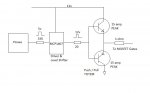
You should see that for fast switching the poor old PIC is way too small for fast switching. PIC will not happily drive that MOSFET at 10kHz.
Read the PDF I posted recently for general driving information, but there is tons available from various Manufacturers. IR produce some good stuff. Then look at Data Sheets for various I.C. drivers.
Spend a few weeks on it and you will get the answers to all your questions :)


OH, it won't let me upload Excel.
Oh well, I'm sure there's an on-line calculator somewhere.
Sorry, I'm afraid I can't give a 100% answer to your question.
 
Last edited:

Dicky Mint

Senior Member
Thanks Dippy Ball park figures are useful but getting down to the nitty gritty is perhaps the best basis for them! Thanks for your post I found it very interesting. Will do some research and circuit testing. Rick
 

Haku

Senior Member
You know that Arthur C Clarke quote about technology & magic, well transistors & MOSFETs to me are magic devices I'm still having trouble getting my head around, often finding it quite frustrating. I wish I could get them working first time & every time like I can do when wiring up the power & programming socket to a Picaxe chip (at least I got that nailed).

I've tried wiring up (again) the NPN+PNP circuit I posted above with a 10v source, replacing the La2 with a single IRFZ46N, and this time it worked and can switch an external 13v source on/off. The NPN+PNP I used are power transistors capable of 3A so I'm going to go ahead and hook it up to a Picaxe, then if that's working I'll hook it up to the capacitor + MOSFETs setup.
 

John West

Senior Member
Here's my bit:

Haku, BJT's (older style transistors) and power MOSFET's aren't too difficult to work with, especially in switching circuits (on/off.)

Some major differences between BJT's and MOSFET's in switching circuits are as follows:

Silicon BJT's (as most are) drop somewhere between .5 Volt and 1 Volt (generally around .7 to .8 volts) no matter how much or how little current flows through them, while MOSFETS drop a voltage that depends on their specified 'on resistance,' just as long as they are fully driven by a sufficiently high gate voltage. Depending on the voltage and current used in the circuit you are designing, one or the other will likely work better, less energy loss, lower drive requirements, etc.

The advantages of using a MOSFET are many, but the low ON resistance is probably the most important one. The disadvantage of using a MOSFET comes into play when you are trying to switch the circuit on and off rapidly. Power MOSFET's have a high gate capacitance, much higher than a typical power BJT. That means that a significant amount of current needs to be fed to the gate to turn it on (charge up the capacitor,) and a significant amount of current needs to be removed from the gate (discharge the capacitor,) to turn it off. This isn't the case so much with BJT's, so they are often selected for high frequency switching needs.

But MOSFET's advantages (especially in low voltage circuits) make them desirable enough that extra effort put into driving them is often worthwhile. If "turn it on for awhile, then turn it off for awhile" speed switching is what you want, then a PICAXE circuit can directly drive most MOSFET's (with reservations.) The heating of a MOSFET (in addition to what will occur due to its stated ON resistance) occurs while the device is being turned on or off. If the PICAXE output is being turned on and off rapidly, the FET input (and output) may spend a lot of time in that gray area between the two. The higher the frequency you try to run them at, the higher the percentage of time they spend in the high resistance gray area between OFF and ON, dissipating heat.

If the circuit driving the gate is just a PICAXE, it has limited current 'source and sink' capability, so if it is running at a high ON/OFF rate it will charge and discharge a large MOSFET's gate capacitance too slowly, and spend forever somewhere in that higher resistance state between off and on, getting hotter and hotter all the while.
That's why there are driver chips for large MOSFET's. They can very quickly charge and discharge the gates of MOSFET's to ensure the outputs snap between ON and OFF quickly.

The other critical item involved in driving MOSFET's is the voltage required to fully turn them on and get the lowest resistance (the specified ON resistance.) For typical MOSFET's that's about 7 to 10 volts, higher than a PICAXE will drive directly. There are MOSFET's designed for 5 Volt drive, and they are often used by folks running 5V circuits, but they are harder to find surplus, (in junk boxes,) cost more for the same ON resistance and will likely have higher gate capacitance for the same power specs as other FET's. There are always trade-offs.

As you already have an array of large high-power MOSFET's, and you know that they can be paralleled (if they are all mounted close together on the same heatsink so they share a common temperature,) then all you have to do is switch that paralleled (summed) gate capacitance On and OFF quickly enough to keep the MOSFET's happy.

There are all sorts of ways of doing that depending on how often (or fast) you need to switch them. The easiest way is to buy a driver chip that is driven by the PICAXE and has enough current source and sink capability to drive the substantial paralleled MOSFET input capacitance fast enough that the gates spend little time between On and OFF.

The cheapest way is to just use a pull-up resistor to 10V or so, of a resistance value the PICAXE can handle, but that means that whenever the PICAXE stops pulling down on the gates, (such as when it's powered off,) the FET's will be ON. Also, with all of the MOSFET's in your circuit, turning them all on would be a very slow process, as the pull-up resistor you select can't be of a value lower than what the PICAXE can pull all the way down. BJT's as a driver stage work better than a direct drive from a PICAXE, but also have problems. The first one is that they don't pull any lower than .7V or so when they turn on, and also you need to both charge and discharge the MOSFET gate capacitance, so active pull-up and pull-down devices are required, making things rapidly more complex. But I could go on and on.

Best to use a driver chip.
- - -
A further point worth noting about MOSFET's is that once the gate has been charged it pretty much stays that way, and almost no current is required to keep them turned on, so the less often they are turned ON/OFF, the more efficient the MOSFET's become relative to BJT's, which require current all the time in order to stay ON.
 
Last edited:

Goeytex

Senior Member
Haku,

You circuit may switch 12v but it is woefully inadequate. While the transistors may be able to switch 3 amps, the 4k7
resistors on the collector of the NPN prevent it from conducting more than a few milliamps. It might as well be a
100 ma signal transistor. Then sending only a few milliamp to the base of the PNP means it can only conduct possibly
100ma max. Bottom line here is that it won't drive the FETs adequately.

I posted a push pull circuit that can drive a few amps and make use of your HP transistors. Take a look at it.

Alternatively you could get a high powered MOSFET driver and stop messing around with designs you don't really have
a grasp on. I think Microchip has a dual 9 amp Mosfet driver that may be adequate.
 
Last edited:

SAborn

Senior Member
One thought here, if you dont have the driver/level shifter that Goeytex shows in his diagram, you could use a good old 555 timer chip in its place, and just use the picaxe to toggle the reset pin, i have used this setup many times with a picaxe as a level shifter with good results.

I think most of us who have done electronics for a while would still have a drawer full of 555's, and wondering what to use them for now we have picaxe chips.
 

John West

Senior Member
While a 555 would require a few extra parts, it would make very easy the setting of a reliable single pulse width output. It also has substantial output drive current, compared to a PICAXE. Seems to me it was on the order of 200 mA, though my memory of such has been fading ever since I started using the PICAXE chips. But if one has a bin full of them gathering dust, they might work nicely in a "one off" project.
 

Goeytex

Senior Member
If you decide to use a MOSFET driver ( highly recommended) a TC4452 from Microchip should do the job nicely.
It can switch a 22,000 pf load in 44 nanoseconds with a peak current of up to 13 amps. SPICE simulation shows that
your FETs will barely get warm using this driver. Cost ? < 2.00 US $
 

Paix

Senior Member
While a 555 would require a few extra parts, it would make very easy the setting of a reliable single pulse width output. It also has substantial output drive current, compared to a PICAXE. Seems to me it was on the order of 200 mA, though my memory of such has been fading ever since I started using the PICAXE chips. But if one has a bin full of them gathering dust, they might work nicely in a "one off" project.
I think that what SABorne refers to is not a pulse, but using the 555 chip as an inverting buffer, by commoning pins 2 and 6, trigger and threshold, with the output from pin 3. Pin 4 reset high. At 5V it should be good for sourcing or sinking 100mA.

Many thanks Goeytex; the recommendation of a TC4452 FET driver will probably save many a lot of grief, maybe even keep Dippy from pulling out all his hair on occasions when dealing with the high frequency of such FET driver questions. In the past there has been a lot of allusions to drivers, but I think (probably incorrectly) you are the first person to give a part number to sate us mere FET-mortals on the forum.
 

Goeytex

Senior Member
Ha,

I have given part numbers before ! The amazing thing is how hard some folks will try to NOT use a FET driver when
it is such an elegant and inexpensive solution to so many problems.

Microchip has the best selection of through hole ( PDIP) FET drivers. They come in dual, inverting, non-inverting &
range from 1 amp peak to 13 amp peak drive capability.

And what a lot of folks may not be aware of is that some of these Microchip FET drivers can sink./source 2.5 amps
continuously and can operate as motor or solenoid drivers.

Below are links to Microchip's Low Side FET drivers in order of current sink/source capability

http://www.microchip.com/ParamChartSearch/chart.aspx?branchID=90101&mid=11&lang=en&pageId=79
http://www.microchip.com/ParamChartSearch/chart.aspx?branchID=90102&mid=11&lang=en&pageId=79
http://www.microchip.com/ParamChartSearch/chart.aspx?branchID=90103&mid=11&lang=en&pageId=79
 
Last edited:

Dippy

Moderator
"Incorrectly" Paix, I gave a part number on the 28th March 2009 at 08:58 if my memory serves me correctly :)


I, too , wouldn't even bother making a discrete setup where the spec wasn't too excessive but where I wanted fast switching.
Horses for Courses.

There are so many drivers* (and many duplicates) that sometimes it is diffcult to name a part especially on those occasions where the application is a little unclear. And ,often , inexperienced people want as fast switching as possible and this is sometimes not desirable. Again, without a clear requirement spec it's difficult to absolutely specify a device and design.

* e.g. get onto Farnell site and search on MOSFET Drivers....
 

Dicky Mint

Senior Member
Just a practical point about MOSFET drivers. What sort of thickness should PCB tracks be made? I'm assuming meaty (!) but not that full thickness that would be required for a constant current of a significant number of amps. I'm thinking that as the large current, needed to charge and discharge the gate capacitance, would only be for a very short period of time, one would not need the track thickness calculated for a constant current of the same value? But I'm not sure, any comments?
 

Dippy

Moderator
Do you really mean "thickness" or do you mean width?
Thicknesses are predtermined by the Manuf. They are usually specced in that wonderful metric unit of Oz.
Best we clear up terminology at the first hurdle.


There are dozens of on-line calculators for track/trace width current and resistance calcs.
Spend 5 minutes Googling.
Easy-PC has a built-in calculator which can do many other things , so download the demo and have a go.


Yes, heat is the killer as usual with just about every aspect of electronics. So, yes, the average current comes into play when deciding width, but err generously on the side of caution. Heavy pulsing an over-thin track , even if your calcs say OK, will not last as long as a fat one. I'll leave the student to ponder why. Just, stay cool.


However, when you get into HF pulse and RF PCB design there is more than just width to consider; inductance for example.
And that needs to be considered in driver PCB design. Widths, proximities and angles need to be thought about in good designs.
For 'good enough' designs just make the tracks short, fat and straight.. and preferably nowhere near signal tracks.


I think it may be good if you have a Google session on MOSFET driver Application Notes.
They will be far clearer than 20 paragraphs of text on a Forum.
So, after Googling the track calculator have a Google for App Notes.
 

Dicky Mint

Senior Member
Thanks again Dippy, yes I did really mean width, bad terminology I accept. I've checked a few online 'track width calculators' in the past and now I use the rule of thumb of 1 mm per amp for 2oz board. Apparently one can calculate the r.m.s. value of current and this apparently gives an indication of current carrying capacity of a trace. I haven't done this yet as I wonder how accurate it would be because the faster a MOSFET switches, the greater the instantaneous current and it is not how long it is on which draws the current. Don't really know where to go from here so I'll do some Googling of App Notes for MOSFETs.
 

Dippy

Moderator
It will be a combination of switching speed and , where appropriate, PWM/switching frequency. Coulombs/second. Do your calcs , x2, . Don't get too caught up in resistance calcs as there are other aspects (as I already mentioned) that should be considered.

Power dissipation in the driver, parasitic inductance , supply capacitance/inductance are aspects to consider too.
I'm afraid it can get complicated, but the simple approach is to keep it fat, short and tight and use the proper components.

Don't get obsessed with ridiculously fast switch times. It's NOT a Land Speed Record, it is a compromise between efficient driving and reduced resonances and RFI/EMI.
I do this kind of thing as a job, by the way, and we had to slow the switching down to comply with EMC regs.

Reading a few MOSFET Driver Data Sheets should give you some good guidance (or "insight" as Stan likes to say).
 

Dicky Mint

Senior Member
ok reading, reading, reading, its a good job I actually enjoy perusing semiconductor datasheets! I've designed a PCB that might do the job I want it for, a six 'bar', therapeutic, ambient, sound-to-light unit based around a PICAXE-14M2. I'd like to show you but I don't know if I can attach "Sprint Layout" files to a post?
 

Dicky Mint

Senior Member
Sorry, I'm really showing my ignorance now. How do I attach a screen print of a jpg? I've never done it that way! I've got as far as putting the screen print on the clipboard.
 

Goeytex

Senior Member
As Dippy touched upon, super fast switching times can many times lead to unacceptable RFI/EMI.

Attached is a schematic that shows one practical and simple way of slowing down either the switch on or
switch off time ( OR BOTH) of a low side MOSFET. I have used this quite a bit over the years.
 

Attachments

eclectic

Moderator
Sorry, I'm really showing my ignorance now. How do I attach a screen print of a jpg? I've never done it that way! I've got as far as putting the screen print on the clipboard.
1. Do a screen capture.

2. Save as or convert to a jpg

3. When you reply, us the
Go Advanced option (lower right)

4. Upload your file after you've solved the mini-puzzles. :)

There are alternative methods, but
Dinosaur me just uses that.

e
 

eclectic

Moderator
Hi I've tried opening the screen print in Paint and attaching it. I hope its not too big?
173 kb is fine.


Just two suggestions here,

1. Attach the schematic.
2. Crop the image to just the essentials.

Which Windows are you using? XP / Vista / 7 ?

e
 

Dicky Mint

Senior Member
View attachment 9455View attachment 9455I'll try and attach a schematic of the electronic part of the circuit. The rest is pretty straightforward a 78L05 voltage regulator, with incumbent capacitors, a PICAXE-14M2 with each B output pin (B.0 to B.5) connected to a MOSFET driver and, in turn, a MOSFET, which turn off and on the custom made LED bulbs.
 

Dippy

Moderator
I haven't got time to check PCB artwork properly but a quick look indicates you haven't read the driver Data Sheet properly.
"The VDD input is the bias supply for the MOSFET driver and is rated for 4.5V to 18V with respect to the ground pin. The VDD input should be bypassed with local ceramic capacitors. The value of these capacitors should be chosen based on the capacitive load that is being driven. A value of 1.0 &#956;F is suggested."

Further hints are given in Figure 4-1 of the Data Sheet (well, in the one I have).

Your FET section layout looks tight, good. It may be fine for your little app. but you haven't taken much notice of our points re: switching times.
Goeytex gave you some hints on gate drive limiting. Sometimes just a simple resistor will do.
If the external load leads are long you may cause interference. Even a gate resistor of 15Ohms may help. That would cut switching down to approx ?00nS and reduce RFI/EMI. S/M is better.

I reckon your driving will work, but as to working ideally is another thing. A lot depends on load.
In any event you're nearly there so I wish you well with your project.

PS. When you want people to check things please post a schematic. Trying to decode artwork is as hard as decoding breadboard images.
 

John West

Senior Member
Dicky Mint, the basic idea of high-speed, high-current voltage transitions creating RF noise is that a square-wave generates all odd-order harmonics of the fundamental frequency of operation, meaning ever higher frequencies of noise being generated, some of which make it out of the switching device via following the wiring or radiating from it, and can interfere with other electronic devices. The fundamental frequency (a sine wave,) generates none. So slowing down the rise and fall times of a switching device "rounds the corners" of the presumed square-wave of an "ON/OFF" waveform, reducing the harmonic content, and thus reducing nuisance stray RF.

There will be a sweet spot in the rise and fall time of the gate that will keep the MOSFET from getting hot (too inefficient,) and you hearing a buzz in everything electrical in your shop and interfering with your neighbor's telly.

But first, you need to get the rise and fall time fast enough to make the MOSFET's happy. After that you can try some resistance in the gate leg to slow things back down a bit. This can nearly all be calculated in advance with enough data and experience, but if you lack such, start by being sure you're driving the FET's quickly, then experiment the rise and fall times back down, with gate resistance and/or other filtration techniques. That's the experimenter's usual method, and it's kinda fun.
 
Last edited:

Dicky Mint

Senior Member
Hi Hansen, I think I know what you're getting at. The load represented by each home-made LED bulbs is about 240mA resulting in a value of less than 1.5 Amps for the six, when they're all on. I'm using the MOSFET BUZ11 for switching the LEDs on and off and they're rated at 30Amps so no difficulty there. I use BUZ11s because I like them, have had experience with them and they seem to be pretty sensitive and bomb proof! The wire I'm using to connect the LED bulbs to the circuit board is colour coded, 10/0.1mm, rated at 0.5 Amps. The ground return is a bit more sturdy and 16/0.2 does the job at a rating of 3Amps.
 

Dicky Mint

Senior Member
So its the corners of the square wave that give the RF noise problems? Or to put it another way the high order harmonics of a square wave cause the RF noise? And the limiting of this high frequency noise is a trade off against the MOSFET being quickly placed in conducting or non-conducting state? A sine wave would produce no RF noise but would keep the MOSFET in the zone where it would be required to dissipate lots and lots of heat! Knocking the corners off a square wave would limit the RF noise but also, hopefully, cause the gate to swing quickly enough to keep the MOSFET mainly out of the heat waste mode. I like the idea of a sweet spot I think I could run with that. To "get the rise and fall time fast enough to make the MOSFET's happy" does this involve sticking a finger on the MOSFET tag and hoping its not too hot to touch?
 

eclectic

Moderator
snipped
. I like the idea of a sweet spot I think I could run with that. To "get the rise and fall time fast enough to make the MOSFET's happy" does this involve sticking a finger on the MOSFET tag and hoping its not too hot to touch?
Seriously, if you're time-rich:

Get a DS18B20 or an NTC thermistor (0.20p)
and do some research by measuring

Frequency vs Temperature.

Then publish the results here.

e
 

Goeytex

Senior Member
Looking at the board layout, I see that 12v comes in at the top middle of the board and 0v (ground) come in at the bottom right.
The pads imply soldered wire connections.

I would suggest moving the 12v input near the 0V input so that a 25v 100uf - 220uf capacitor can be placed across them.
Then add a 1uf capacitor from the 12v connection of the Regulator to ground. These changes should help to stabilize both
the 12v and 5 volt supplies.

As far as the switching time, here's what I would do. Put 20 ohm resistors in series from the driver output to the FET
gates. Then if there is an issue with excessive noise, increase the resistor value. This really does not to have to be
that complicated.
 
Last edited:

Dippy

Moderator
"So its the corners of the square wave that give the RF noise problems? Or to put it another way the high order harmonics of a square wave cause the RF noise? And the limiting of this high frequency noise is a trade off against the MOSFET being quickly placed in conducting or non-conducting state?"
- short answer ... yes.

Hence the suggestions, where needed, of the gate resistor.
Remember RC charge/discharge curves? As you know the Gate is a capacitor, therefore.....
And a resistor can often help with nasty resonances as it can damp.(LCR).
These things are often difficult to measure properly with cheapo 'scopes.


As to the effect of 'slowing' the gate charge/discharge; imagine a PWM 50% duty square wave. A very slow charge/discharge makes this trapezoidal-ish with leading and trailing edge triangles. The area in the triangle represents the heat generated in the 'resistor' zone of the MOSFET. I think I said all this before??
And like I said before; MOSFET driving is a COMPROMISE between efficient switching and noise.

I really don't think 200nS switching time will have much effect on the baby currents you are opertaing at and at the frequencies mentioned previously. After all , what proportion of your wave is a 200nS resistive bit (even assuming worst case)?


"To "get the rise and fall time fast enough to make the MOSFET's happy" does this involve sticking a finger on the MOSFET tag and hoping its not too hot to touch? "
- unless you have a thermal imager or IR thermometer, yes.
The calibrated thumbometer can be very useful :)
 
Top