DIPTRACE smd parts for smd picaxe's

manie

Senior Member
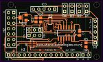
Which DIPTRACE layout component parts to use for:
1. SMD 40x2 (QFP-44 ?)
2. SMD 28x2 (SOIC or mil-300 ?)

I would like to start playing with these SMD components and professionally made double-sided boards.
This subject I know VERY LITTLE of !!!!!!!!!!!!!

Can anyone help ?

EDIT: add some parts

I will also use the following parts:
1. LM2931 linear LDO regulator
2. 470uF and 220uF electrolytic caps - the IPC7351 CAPUD83
3. 100nF cap the CAP6032T
4. For resistors I think I will use the RES-SMD CR0805's
5. Diodes like 4001-4007 the DIODE-SMD sod-2.4/w4.8 outline OR
the MELF-D1406 or the CD1306 outlines

What do you think or what do you use ?

Thanks in advance
 
Last edited:

Svejk

Senior Member
Manie, you'll find most of footprints under "General" library. When you draw your schematic just change the "attached pattern" of discreetes/ic's etc to whatever are you using. A better approach would be the use the ready made smd libraries in Schematic editor.
 

srnet

Senior Member
I wouldd stick to the SOIC, and it is the only SMT package the 28X2 is available in.

I was told that REV-Ed would be prepared (for a fee) to program a native PIC (18F25K22 in this case) with the PICAXE firmware if the PCB provided a PICKIT or TAG CONNECT programming header. DIY soldering of the QFN packages is really for the experinced constructor. The SOIC SMT is not difficult for the average constructor, although quite a lot bigger.

You would also likley find hand soldering of 0603 and 0805 components (resistors & capacitors) quite difficult, unlesss the finished board size must be really small I would stick to 1206, at least you can see these when you 'missplace them'
 

manie

Senior Member
@ Svejk: The "General"library is through hole stuff, not SMT........

@ srnet: The QFN 40 I did find. The 28pin SOIC package is available in MANY sizes. The 28x2 is of the 300mil SOIC type, but where to find the footprint in DIPTRACE.
It is all still abit confusing......

I drew up a footprint for the ULN2803 SOIC from datasheet. The two rows of pins are spaced now at 9.5mm and not 9.4mm like the datasheet says. Does that small
difference matter ?

Thanks for the replys so far...........
 

Svejk

Senior Member
Manie, maybe is time to update libraries? My "General" build this:

smd_boad.jpg

PCB Layout, v. 2.1.9.5 (beta)
 

Dippy

Moderator
"The two rows of pins are spaced now at 9.5mm and not 9.4mm like the datasheet says. Does that small difference matter ?"
I doubt it. I assume you've made your lands (SMD pad area) a little larger than the pad contact points?
Some data sheets also give recommended land sizes and positions.

If your Data Sheet only gives pin contact dimensions then make the land/pads larger. I assume you've made the land/pad as square fingers (rectangles)? make them generous in the longer dimension.(Without going daft obviously).
There are a couple of good reasons for this. With home soldering you may have to give extra heat so a larger pad has a better chance of staying stuck to the board, and a larger pad will allow more shakey-hand tolerance and allow you to get solder in.

If this is your first go, I would thoroughly suggest getting the components FIRST and then you can actually see what is going on AND it allows you to print your artwork onto PAPER and plonk the components on it to check alignment BEFORE doing the pukka PCB.
 

manie

Senior Member
Svejk, this is the NEW download from Diptrace, V 2.1.0.7, not the beta version though. It is a paid for Diptrace Lite version. It shows through hole stuff.
Did you change the pads to surface mount with holes ?
 

srnet

Senior Member
I use EAGLE PCB, and there is a PICAXE library for it, the 28X2 SOIC from there is the correct one. Interestingly though the 20X2 uses the wrong package (SSOP) so I got the 20pin SOIC from the Microchip library.

Completly agree with what Dippy says, you really do need the components in your hand to check them out. The dimemsions of the 28X2 SOIC will be found at the end of the 18F25K22 datasheet, so you can check the library part matches the datasheet.

Whilst the differance between 9.5mm and 9.4mm is small, if you know its wrong why not just correct the error, DIPTRACE I dont know, but correcting that sort of error in Eagle would take a couple of mins.
 

manie

Senior Member
Dippy, hoped to get you on-board. Firstly, the board is as per post #1, professionally made and "picked and placed".
I very much doubt I will EVER try a home-made SMT board, I mean I need a magnifier WITH glasses for some through
hole stuff already !!!! Yes, the lands are rectangular but as per datasheet (for ULN2803A). You don't use Diptrace
(said so yourself) but yes I get the point about getting the stuff first for the final layout !!

This is my FIRST try with SMT and double sided board so right now I am playing around "to see..."
 

manie

Senior Member
srnet, good tip re getting the sizes from the datasheet. I suppose I could add 0.1/0.2/0.4 etc to the grid pattern, now it is from inches
where 0.1 inch = 2.54mm........ I will try that.

That is why this forum remains SO GOOD ! Look at the responses.......
 

srnet

Senior Member
If parts are quoted for 2.54mm pads, I place them using a 0.1" grid and then swap to a 0.1mm grid for drawing the physical part outlines.
 

nbw

Senior Member
SMT isn't actually too bad. I too used to be of the "if I can't read the marking easily, I can't solder it" variety. A toothpick, a mini-dab of flux and a dab of solder-paste, tweezer that component on there... add a sip of brandy and 30 seconds of gentle waving with a hot air gun. "Big" ICs like the SMD 08M are luxury now :)

I make my PCBs using Diptrace and always print a paper copy out, then lay the components on before ironing, etching etc.
 

srnet

Senior Member
I have been laying something out for a 20X2 using 1206 resistors and capacitors.

Assembly of the 1206 size should be within the capability of most constructors. No need for ovens, hotplates or similar. The component and PCB pads should be already tinned. If you hold the 1206 component in place and touch the pad with the iron, there is enough solder there to tack the component in place, you then just use very fine wired solder to make a proper joint at either end. Same goes for SOIC ICs.

I would use wired components but there is a substantial differance in size between a wired 1uF ceramic and the 1206, 0805 or 0603 equivalent (needed for regulators). Same goes for small electrolytics, tants and LEDs.
 

Dippy

Moderator
There are many hints and tips on producing home-made SMT PCBs.
Maybe someone should write a Tutorial with an appropriate and accurate heading/title.

In this case Manie has said: "Firstly, the board is as per post #1, professionally made and "picked and placed".
- so he won't need this wise advice.

If the advice is aimed at a general audience then a Tutorial/Blog may be a better place. I, for one, have heard most of the sensible hints and tips given above numerous times, so a central rememberable/accessible place would seem a better place.

These days I just get the Butler to make mine :)
 

manie

Senior Member
I am only now starting toreally use DIPTRACE with this SMT stuff. Everything is going that way anyway, just look at MAXIM ! Hardly any throughhole stuff there !
I guess sooner or later we all have to migrate to SMT and professionally made boards or what ?
The DIPTRACE auto router is not that great........ leaves a few blue lines for you to route manually.
Or is MY layout and placements ?
 

manie

Senior Member
One more question on manual 1.

The 44 pin QFP for the 40x2 does not show any HSERIN or HSEROUT pins.
Are they there and which pins ?
 

srnet

Senior Member
It says on the 44pin 40x2 diagram "please see DIL pinout for individual pin functions"

HSERIN is c.7 and Hserout is c.6.
 
Top