Designing and building PCBs

Dicky Mint

Senior Member
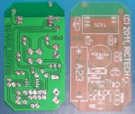
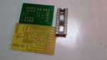
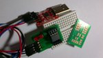
Hi I'm an enthusiastic PCB designer and builder using the 'Sprint Layout' software.

I would like to gain some experience in designing and building single and double sided PCBs.

I have the intention of eventually making a modest profit but at first I am looking to gain some experience by fabricating boards for cost.

I don't know if there is any call here for bespoke PCBs from circuit diagrams or even first concept prototypes but you don't know 'till you ask!

My perspective is that I enjoy coming up with prototypes of electronic solutions to engineering problems and would like, one day, to make a modest living in this area.

Rick
 

geoff07

Senior Member
Questions, questions .. I'm sure many would like to have a low cost board fab process (one-off boards are expensive to have made professionally)

Are you planning to etch and drill the boards yourself?

Could you use other design software e.g. if I used Eagle to design a board, could you fabricate from the BRD file?

Are you planning to populate the boards and test them?
 

Dicky Mint

Senior Member
Hi geoff

First question first, yes I'm planning to etch and drill the boards and with Favorit rivets for plated through holes!

The second question is one which I'm sure will come up a lot but at the moment the answer is 'no' as I have been more interested in the design process than the etching, forgive me but I love Sprint Layout! It would certainly be useful for me to be able to make boards from BRD files and Gerbers so I will look into these possibilities if there s call for it.

As for populating and testing, if that were something which was required there would be no reason why not although my itinerary of test equipment could do with an overhaul! I think this service would bring with it its own quota of problems though not insurmountable, I hope.

As you've probably gathered its a work in progress but 'from Acorns...'

Rick
 

SAborn

Senior Member
If its just small numbers of not over large boards involved, it would be best to let the client assemble the boards and test them but offer a free replacement should YOU have got the design wrong, as its much faster for you to make a design change and redo the board than dick around with assembly and testing.

A small cnc machine would be worth its weight in gold for drilling the boards, but be warned if you are printing the artwork out and exposing it on to the pcb, then all printers of today have counterfeiting errors programmed into them, and move the image around slightly to the original design, although this is not enough for a circuit not to work, but it will misaligned the holes for the cnc machine.

It took me months to work out why my machine would drill fine for some boards and then be 1/2 a hole out on others, or some of the board would be perfect and a section or two would drill slightly out.
I thought i or the cnc was goinig mad (it was driving me mad) but ended up being the printer losing the plot (punt intended)

Will Sprint allow you to create and export a drill code (Gcode) for a design, if not then its not worth getting to reliant on it, as if you do high numbers of boards you will need a way to drill them, and a cnc works while you are doing more important tasks, like coffee or design work, etching etc.
 

Dicky Mint

Senior Member
Hi SAborn

A CNC machine would be a desirable addition but not one I could consider at the present time. I use a Dremel and a drill press at the moment.

I didn't know about the printer anti-counterfeiting measures which could potentially cause problems.

Sprint exports a 'Excellon' file for drill holes or a Gerber export although I must confess I have not used either.

Other PCB software I've used doesn't seem to produce an elegance half as good as my trusty Sprint Layout though.

Rick
 

Janne

Senior Member
SAborn,

Interesting information re. the new printers. Think I'll hold on to my trusty old HP 5L for printing 1:1 cutting templates and PCB's :)
 

WHITEKNUCKLES

New Member
Rick,
I wish you success with your enterprise.

Am I right in thinking that if you were sent a pencil sketch of a circuit diagram (perhaps with intended layout) that you would produce an etched and drilled board?
That is provided that they supply you with a Bill Of Materials showing the pin spacing of each component such as~~

Q1........................08M2 DIL
R1 to R8................0.4"
C1,C4....................0.2"
Etc.....................

Would you provide a printed version for approval?

Dave
 

Grogster

Senior Member
I use Sprint Layout for all my boards(I know some of you don't like that app, but...), and I can either make prototypes here at home, or send the .LAY files for professional manufacture. I use Futurlec to make my boards:

http://www.futurlec.com.au/PCBService.jsp

Just select what you want, and choose Sprint Layout from the drop-down list of programs.

They are just fine for multiple boards, but as already mentioned, not really economic for one-off's, so I always make the prototypes here at home, and once I am happy the layout is correct and the prototype is working as expected, then I order the boards. See attached photo of boards made by Futurlec for one of my projects(now abandoned). This board used the SMD PICAXE 08M chip.

I have made hundreds of PCB's here at home.
I would be happy to upload my method if you want to see how - I am sure it is pretty common.
 

Attachments

Last edited:

Goeytex

Senior Member
all printers of today have counterfeiting errors programmed into them....
A Google search offers no evidence of this as an indisputable fact. Where can I find a credible source of information that supports this? When was this implemented?
 

Dicky Mint

Senior Member
Hi Dave

Yes that would be that, that I could do, to produce a PCB from a circuit diagram and pin spacings.

Holes would be 0.8 mm or 1.0 mm, I've found 0.8mm most suitable for leaded components, Rs, Cs, Transistors etc.

1.0 mm are suitable for small presets, off board terminals, and larger semiconductors (eg T0220) etc.

Also I often use 2.5 mm or 5mm pin spacing for capacitors and 8mm or 10mm for resistors, various spacing for electrolytics based on electronics catalogue.

Any of these can be altered if desired but these have passed the tests of time.

and yes I could provide a printout for perusal prior to producing a PCB.

Rick
 

MartinM57

Moderator
That may be true (I'm sure it is) but the question is about printers having random(?) errors built into them means that holes and pads on a PCB image don't align properly...
 

SAborn

Senior Member
Even though an IC pad will be slightly out in the printing its not enough to prevent the IC fitting into the holes if they are hand drilled to the printout, you would never notice the error in the printing unless you try a exact X,Y plot over the graphics from the original design, like the cnc will do from the design Gcode.

There must be a size limit before the printer error is implymented as all small board designs are not effected and i suspect its a size of around a bank note upwards that the error is introduced.

I dont recall a website to point anyone to0, to confirm the printer error, but it was pointed out to me on another forum by a person who worked in printer design, and was given web information to confirm the claim, so it is on the net but i dont know where now.
From what i recall it has been in place for around 10 years or more and most likely when the first colour printers were introduced.

One thing i dont know and want to find out, is if this error applies to mono chrome printers also, as who needs colour to print circuit artwork, and i am waiting for my colour laser printer to run out of toner, then its getting the boot and being replaced by a mono chrome printer to find out if the error is still present.
 

Goeytex

Senior Member
@Goeytex. Try scanning a banknote. My Epson software sends me here

http://www.rulesforuse.org/pub/index.php?lang=en

R.


CDS would not come into play unless a protected banknote was scanned / copied. There is no mention of random errors being generated by printers when printing non protected documents & images.

I am interested in where the information came from that random errors are generated regardless of what is being printed. I have several HP Color Printers and a OKI Color Laser Printer & I have never had a problem with random image shift / registration when printing board layouts, registration marks, holes, etc.
 

Dicky Mint

Senior Member
Hi

I have a monochrome Laser printer and align top and bottom of double-sided PCB artwork by eye. I haven't noticed a misalignment of parts of the artwork. I'll keep my eyes open but hope this is not an issue for monochrome lasers.
 

Armp

Senior Member
From my days at EPSON R&D - there are features in some SCANNERS and COPIERS to prevent counterfeiting.
There are none that I know of in the printers.
 

Paix

Senior Member
Around 10 years ago I remember reading about yellow pixels being placed on pages to forensically identify colour printers used, (in the printing of leaked documents for example?). To find them you would need to look with magnifiying equipment and presumably filters to enhance the dots. It was widely reported at the time and I think may have been printer/s from HP.

About 7 or 8 years ago a friend had mentioned that a new scanner that he had purchased, scanned a £10 note to see how well it worked, balked and issued a warning on the LCD window that what he was trying to do was illegal. He was quite taken aback and wondered about what else his scanner might be doing!

I did wonder about an Epson printer that gave me a right run-around when using non-Epson ink cartridges. I felt that the behavior had probably been programmed, so that I would become extremely disenchanted with the performance of third party cartridges. In fact I almost felt like throwing the whole printer through the window and replaced it within the week with a Samsung monochrome laser printer which has behaved beautifully for six or seven years now.

Google "printer yellow dots" for reams of info about the dots.
http://w2.eff.org/Privacy/printers/docucolor/
 

Paix

Senior Member
Duplicated post.

This came about when during a long post a dialogue came up when committing, asking if I was sure that I wanted to navigate away from the current page. I confirmed OK and voila, a duplicated post.
 
Last edited:

pbaker21

Senior Member
I'm using ExpressPCB and it would be a dream to print directly onto the circuit board. For example http://www.youtube.com/watch?v=IG9KNDvoRl4&feature=related

So, how 'easy' would it be using PICAXE(s) to build a plotter to draw onto circuit boards?

* I'd guess for a starter you'd need a couple of servo motors for x and y coordinates and something like a solenoid actuator to control the pen up/down.

The big deal for me is, how to translate info from the PC printer port to the servos via a picaxe. If anyone has any thoughts on this please let me know?? ;)
 

bfgstew

Senior Member
Hopefully I shall be making my first PCB in the next few days/nights, will keep posted on results.
 

pbaker21

Senior Member
Hopefully I shall be making my first PCB in the next few days/nights, will keep posted on results.

Please do! :D

Do you (does anyone?) know how to read and translate data from the printer port of a PC to a picaxe which can control stepper motors? I'd like to be able to understand what goes on there. I would imagine you'd have to create the printer driver software to interact with a Picaxe which then goes on to control the motor(s).
 

JimPerry

Senior Member
Not an easy task - PCB manufacturers use "Gerber" files as a standard. Think about it :rolleyes: - is your printer an Epson, Brother, GP, PDF, Teletype etc etc Plus printers only interact by asking for ink or paper - they don't care what is being printed
 

beb101

Senior Member
Here are a couple of single-sided DIY PCBs that I finished a while back using toner transfer. The one with solder mask is a 08m2 with a non-inverted serial interface and the other a DS3231 RTC clock with battery backup.

Baxter
 

Attachments

Jakob2803

Senior Member
Here are a couple of single-sided DIY PCBs that I finished a while back using toner transfer. The one with solder mask is a 08m2 with a non-inverted serial interface and the other a DS3231 RTC clock with battery backup.

Baxter
Very nice, my toner transfers always suck. :eek:
 

beb101

Senior Member
@flyingnunrt

It's dry film solder mask,

http://www.megauk.com/datasheets/5101_Data_Sheet_Dry_Film_Solder_Mask(500-195-1 & 500-195-2)(0812)(v8).pdf

I bought about 2 feet of it from a London eBay seller. For some strange reason, it is impossible to buy it in the USA in small quantities, but readily available in Europe.

Just follow the directions in the reference to laminate it. I use free Eagle Cad. For for single sided boards, I print the bStop layer on a laserjet transparency. Then, align the image with the pads, tape it securely and expose with UV. I use this exposure frame to keep the image pressed tightly against the board,

http://www.store.cbridge.com/mm5/merchant.mvc?Screen=PROD&Store_Code=TCBPS&Product_Code=CNT-FRM-001-2&Category_Code=FRM

The exposure unit doesn't need to be anything fancy. I use a compact fluorescent 25Watt Damar H25SL/BLB black light blue bulb in a parabolic shop light reflector. This bulb has a spectrum with a peak at 352nm which is nearly ideal (365nm) for exposing photoresists. Position the the board about 5" under the reflector and expose for 3 to 3 1/2 min. YMMV here depending upon your exposure unit. I left a board for 7 min and I couldn't remove the resist from the pads.

After exposure let the board rest about 10-20 min. away from the UV. Then remove the second layer of protective film. Remove the resist from the pads by brushing with a toothbrush or throwaway paint brush in a dish with a solution (10 grams/liter) of sodium carbonate (washing soda). Finally, wash and dry the board and re-expose for 60 min to complete the cross-linking of the polymer. I found that the dry film solder mask is not at all sensitive to regular room light (not too bright) so you don't need any dark-room setup to process it.

Baxter
 

pbaker21

Senior Member
Not an easy task - PCB manufacturers use "Gerber" files as a standard. Think about it :rolleyes: - is your printer an Epson, Brother, GP, PDF, Teletype etc etc Plus printers only interact by asking for ink or paper - they don't care what is being printed
I'm guessing it wouldn't be easy :confused:

How about then building a plotter device that can read data directly from a scanner?
So you initially print out your circuit design on your printer then, pop it into your scanner which is linked somehow to the plotter (via a PICAXE circuit, whatever that maybe) and have it scan and plot at the same time?

Just a thought...!
 

marzan

Senior Member
I would be happy to upload my method if you want to see how - I am sure it is pretty common.
Always interested to see how others do it - especially solder masking. I cant get the hang of it.

Marz.
 

Jakob2803

Senior Member
How do I improve my toner transfers? :) The problem is that when I peel them the ink comes off too. I am using sandpaper before transferring, 300 grit I think. I would have used higher but it was what they had at the store. After sanding I clean it with acetone. After transferring I put the boards in water for a few minutes before peeling them.
 

Jeremy Harris

Senior Member
I found the toner transfer method to be very fussy about the paper used, and other factors, like the iron temperature and the amount of pressure applied are also quite critical. Cleaning the copper is important, but not super-critical; I've had great results with nothing more than giving the copper a quick wipe with solvent first, just to get the grease off. I'd avoid using harsh abrasives, nothing coarser that a Scotchbrite pad (or ordinary pan scourer type pad).

The method I use is to print on the cheapest photo paper I can find, usually the thin, slightly glossy, Staples own brand budget paper. The printer needs to be set to print on to coated paper, I've found. Ordinary printer paper doesn't work at all well, but some have reported that pages cut from old glossy magazines work well (I've not tried this because of the risk of jamming the printer up).

Once the paper has a good print on it I iron it to the copper face of the board using a lot of pressure, with the iron set to its maximum temperature. I've found that it's best to put a pad of paper under the board when ironing it, to allow the board to heat up well. A fair bit of pressure is needed, and once the toner has started to stick well to the copper, carefully rub the tip of the iron over all the trace areas, to make sure they are all bonded down well. Take care not to allow the paper to slip when doing this, or the traces will be blurred.

Once the paper is ironed on well, let it cool, then soak it for ten minutes or so in cool water. I've found that adding a drop of detergent to the water helps it wet the paper, as does lightly abrading the back of the paper with a scouring pad (this lets the water soak in more readily). The paper will rarely peel away cleanly in one piece, I've found, and it's usually necessary to rub bits of stuck paper off with your fingers (taking care not to scratch the toner) under a trickle of running water.
 

SAborn

Senior Member
If you print onto the waxy side of the backing paper laser print labels are stuck to, (the bit you throw in the bin) then iron it down as Jeremy explains above, then place the board in the freezer to cool down (or wait a hour at room temp) once cold the waxy paper will peel away 100% clean without needing to wet it at all, but it must be cold before peeling.
 

beb101

Senior Member
@bluejets

That is a nice wrieup, but I should point out that his method method for solder mask is cosmetic. Green TRF is used to seal voids in the transferred toner so that you do not get pinholes in traces during the etching process. It is not heat resistant. There is a product called Bungard Green Coat that looks to be promising for DIY boards,

http://bungard.de/index.php?option=com_content&task=view&id=65&Itemid=46&lang=english

I have not tried it; you cannot buy it in the USA and I refuse to pay shipping costs equal to or greater than the cost of the product.

Baxter
 

Dippy

Moderator
As this crops up so often it's yet another subject for the Tutorial section.

DEK make some nice screen printing stuf for PCBs. :)
 

beb101

Senior Member
The company cited in one of my earlier posts has a PCB application tutorial,

http://www.cbridge.com/howtos/printedcircuitboard.shtml

I bought one of their starter kits ($25) and some extra photosensitive stencil material. It is very easy to work with and the nice thing is that the development and washout of the screen is water based. Moreover, with this system you can basically do an almost professional board; first, create the basic stencil for the circuit to be etched, next create another for the solder mask using Pebeo Vitrea 160 paint and finally one for the silkscreen. All three screens are reusable if you wash them out before the paint dries. I found, however, that the hard part is laying the paint down through the screen. Viscosity of the paint and manipulating the squeegee is everything here and I could never develop the technique for repeatability.

Baxter
 

SAborn

Senior Member
The question is why do you need to go to all that trouble for a little board you are likely to shove in a box and never see again.
I dont see how a solder mask makes it work any better, if its protection wanted, tinning the board will do more or a good coat of board lacquer after assembly.
 
Top