Critique my PCB design.

Shafto

Senior Member
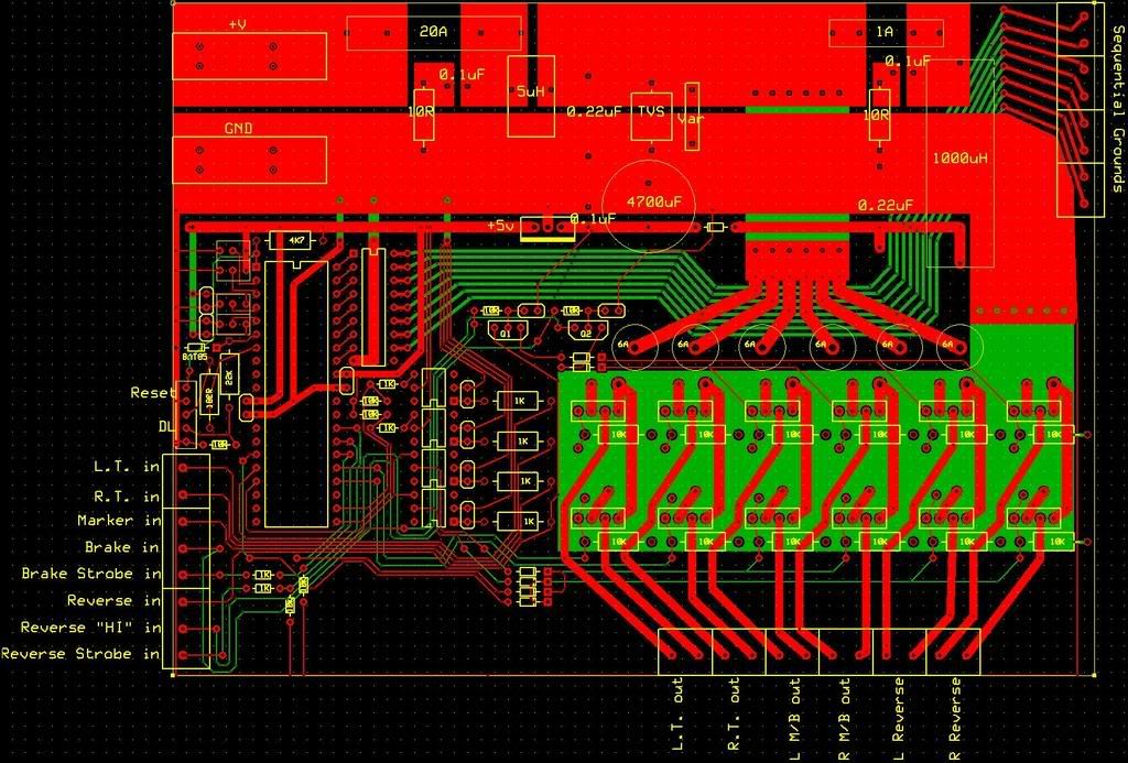
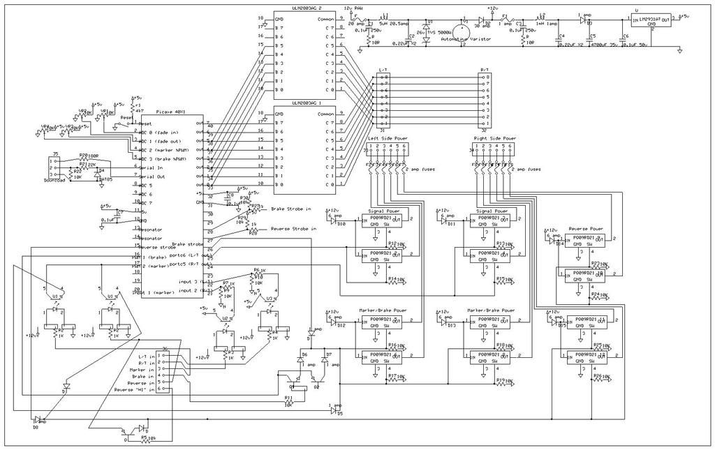
I haven't fully reviewed it myself yet, but it's been a while since I've posted about my project so I thought throw it up.. I've updated the schematic aswell.. but it's gotten somewhat messy now with all the changes.

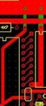
I've never designed a PCB before.. I tried not to daisy chain any power lines and pretty much just did what I thought was logical, I'm sure it's quite unorthodox.

I'm making the PCB myself, so I can't do plate through vias or anything, my 'vias' will just be wire soldered from one side of the board to the other.. in some places where I have resistors connecting from one layer to another I don't have this extra "via" because I figure I can just solder the lead from those resistors onto the top layer/component side (green) quite easily.. not something that would be as easy to do with DIP... hope that makes sense.

The design notes and updates include:

No code switching for the marker lights now.. the PWM signal will run constantly in the background and when the opto-isolator for the Markers is energized it will just conduct the PWM signal to the V-regs.. don't know why I just didn't do it that way before.

No jumpers for negative/positive switching.. it's all positive switched, I tested it out, so I might as well save the board space.

Brake strobe/Reverse strobe inputs are pulled high.. that way I can just run 1 wire to the front of the vehicle and ground it out to activate those inputs.

The LED reverse Lights I made are over 1000lumen each (bright than a 55w halogen headlamp) so they need to be dimmed for city use.. when reverse is activated the opto-isolator conducts the same PWM signal used for the Markers to the reverse lights.. Q1 is a PNP resistor that will be negatively switched up front (Reverse high in).. it takes the "reverse in" signal if present and just feeds it right to the V-regs for full brightness.

Q2 is an NPN transistor that conducts the brake PWM signal to the V-regs, I use a transistor here for faster switching of the brakes than an opto could provide.. trivial maybe.. more effective none-the-less.

I put 0.1uF caps on the inputs to the transistors and the opto-isolators.. I never had this in my schematic, but it seems like a good idea to stop noise from causing false triggers?.. I may use 0.01uF here as I have quite a few extras.. but I'll go with 0.1uF for the picaxe and such.

Something else I thought of I'd like to hear an opinion or 2 about.. should I use a 16V zener diode for the input to the NPN transistor? what about a regular diode on the PNP input?

The only place I ended up using wire links is on the #4 pins of the V-regs (they're upside down #4 is in the #1 position) to link them together.

So set me straight if I've gone astray here.. any input much appreciated :)


Last edited:

andrewpro

New Member
I didn't spend a lot of time looking it over, but it's not too bad for your first time.

One thing I did notice is that you bounce between layers an awful lot where ti's not necessary. Two points that stand out to me are the "sequential grounds" and the chip on the left has a through hole bringing the bottom trace to the top, but it's not crossing any bottom layer traces after it does this.

For the former, I'd just make them all bottom traces out to the holes on the edge. For the latter, just leave it on the bottom of the board.

If I understand your project and it's workings correctly, it wont make a very large deal now, but later on with other boards things like added capacitance and inductance from the constant travel between layers can cause all kinds of havoc.


--Andy P
 

Shafto

Senior Member
I didn't think anyone would go through my connections or take a lot of time.. I just mean the general design.

The traces out to the sequential grounds are switched back to red (bottom) so the components can all be on the same side.

The diagram is like looking at the board from the bottom, the green traces will be on the top side with the components.. I'm not sure if my terminology is correct here because the program I have confuses me, it called green bottom and red top.. I don't really car how it's all named though as long as it all matches up when I print it out :)

The latter layer switching you are talking about I don't quite understand... what's "the chip on the left" ?
 

moxhamj

New Member
It looks very good. The external connections at the bottom left and top right - are they screw terminals? If so, maybe make the pads a bit bigger. How are you drilling the holes - with a 1mm or 0.8mm drill or smaller? You might want to do a tiny piece of board as a test and etch it and then try drilling it just to get a feel for how small the holes should be.
 

BCJKiwi

Senior Member
Re the top vs bottom traces;
If you have boards made out with Through Hole Plating (THP) to bring the traces through, then you might as well have pads both sides at all connections. Then the traces can stay on the same side and you can still make the solder connections on the other side.

If, however the board is not made outside with THP and you have to solder in a wire through the hole to join top and bottom traces, then you should probably stick with what you have.

Andypro's comments also hold for the GNDs to the two ICs on the left and a few of the connections to the 40X1.

The circuit only shows one 18 Pin IC - presumably the ULN2803 - was this the thing where you were going to stack them one on top of the other? - else you're missing a socket.
 

Shafto

Senior Member
I bought a watch making drill bit set, 0.3-1mm in 0.05mm increments, and then the old 1/16" for big holes.. Those are screw terminals yes.. I should increase the pad size.

The 18pin IC is the ULN2803, and there are 2 stacked there for parallel operation.

I'm making the board myself.. so there's won't be any THP.


What are "the 2 ICs on the left"? to the left of the picaxe there are 4 pots, 2 of them have input caps.. the other 2 don't matter if they bounce around a bit.. then there are the 6pin dips which are opto isolators.. I'm not really sure what exactly you and andy are talking about.


I only see one place where I've brought traces to the other layer without anything being in the way.. and that's for the sequential grounds out.. if I left them on the top side I've have to put the screw terminals on the bottom of the board.. and I'd rather not do that.

Concerning the caps on the optos and the transistors.. is this a good idea? and should I be using a zener on the NPN and a regular diode on the PNP ?
 
Last edited:

BCJKiwi

Senior Member
We mean around the 40X1 and ULN2803.

The traces can stay green - provided you have a pad on the red side and the holes are plated through so green and red are connected through the hole the component is installed into.
 

Attachments

Last edited:

Shafto

Senior Member
Ok.. I see what you mean... it's not plated through though.. so I'd have to SMT the dip package.. easier to just transfer back to the other layer.. some of the resistors and diodes I didn't bother to do this because it will be easy to solder them onto the top surface without a plate through hole.
 

Shafto

Senior Member
everything works on the breadboard except some flickering I'm still getting on the LEDs with the PWM signal.. but that can fixed with proper coding.. if i use a solid value instead of a variable I get no flicker..

can someone confirm that the capacitors on transistors and opto-isolators is a good idea? ...this isn't on a breadboard, but I thought it would be a good to stop random triggers from noise... but I dunno? am I right?
 
Last edited:

Shack

Member
I don't think your PCB will work.

It is not laid out for a single sided board. You're saying you are going to mount the IC's on the bottom .... it will be interesting to see how you solder them. If you put them on the top they will be mirrored. Several of the components don’t appear to be connected
 

moxhamj

New Member
Re "everything works on the breadboard except some flickering I'm still getting on the LEDs with the PWM signal.. but that can fixed with proper coding"

Murphy's law says that if you don't fix this first on the breadboard, this will be the one problem on a PCB that will end up being impossible to fix.

I usually do breadboard first, then protoboard with point to point wiring and the components laid out in roughly the same way as the final PCB, and then PCB last. There are always minor faults that need fixing along the way.
 

Shafto

Senior Member
After you breadboard you solder everything onto perf board? then desolder it all and put it on a proper PCB?

...I will sort out the issue first with the code on the breadboard, but the fact that using a solid value on the micro in the breadboard makes for no issues.. then I'm sure it's just programming that can be solved with some proper hysteresis coding.. if I can ever figure it out.

The pots are as close as they can be to the ADC inputs and +v/GND.. so I don't really see anything I can do to improve the physical layout to help the flickering... but I do hate murphy and his fun little law.. so I'll get it working perfectly on the breadboard here before I start etching..
 

moxhamj

New Member
I solder it up using sockets for all the ICs. For passive components I leave them on the prototype and use different ones on the PCB - a bit wasteful I know but I have a collection now of old boards and I end up recycling the components from other boards so I rarely have to buy new components. Then I have a prototype board with sockets and if the PCB doesn't work I can swap the chips back into the prototype and see if it works there and then it makes finding errors a lot easier.
 

inglewoodpete

Senior Member
Shafto, You say you will make the PCB yourself. Depending on the method you use to create the double sided PCB, it can be quite difficult to align the 2 pattern very accurately. This affects the positioning and drilling of the holes for your wire-vias. I suggest you use larger donuts (pads) for any vias to allow for potential misalignment.
 

Shafto

Senior Member
I'm doing the laser print and iron on method. I'm pretty confident I'll be able to line it up nicely on both sides.
 

Mycroft2152

Senior Member
Just some thoughts....

12 voltage regulators? That seems a bit of an overkill. Are you just using these as switches because you have them/

Do all your light / markers run off 5 volts? Most auto bulbs are happy with 12 volts.

Split the pcb into 2 separate boards. The picaxe and logic on one board and all the voltage reguators (drivers) on a second.

Plan on heat sinks.

Post the schematic and pcb files, that would make it easier for somene to clean up.

If you have never made a pcb before,start with a simple one, like an 08M project. There is a technique to be mastered.

Good luck,have fun

Myc
 

Shafto

Senior Member
Shack, The components will be mounted to the "green side" the "red side" will be the bottom/solder side...

I've printed it out onto cellulose so I could see how both sides interact with each other.. all connections are made, you're perception of the design isn't quite correct. I don't know if this will help or be more confusing.. but you have to picture it like you're looking through the top side to the red... when I print out the red side it doesn't need to be mirrored first because it will mirror itself as I put it onto the bottom side of the board... the top side will need to be mirrored before it's printed so it will be the right way on the board... I've never done a PCB before like I say.. but one thing I am good at in general is layout/drafting..


Myo,

They are 9v regs, not for bulbs, custom LED arrays I've already built. I will be putting small heatsinks on the v-regs, but they'll be pretty happy each not running over 1100mA with a max of 2000mA.

1 board works better for mounting in my situation, if i built a second board it would just be right beside the the first one connected with wires instead of traces, what's the difference? I've still separated the logic area and power area on the board.
 
Last edited:

moxhamj

New Member
I'd second profmason's comments but of course, PCBs look more professional.

Have you read http://www.instructables.com/id/Turn-your-EAGLE-schematic-into-a-PCB/ and http://www.instructables.com/id/Make-hobbyist-PCBs-with-professional-CAD-tools-by-/

There are lots of hints on making tracks wider and holes bigger. I have bought numerous PCB kits over the years and a few months back I got all keen about it again and drew up a circuit and laser printed it and ironed it on. It didn't quite work out as expected. There was undermining of narrow tracks by the etchant and some bits didn't iron as well. Then I tried drilling (with a drill press) and I realised all the holes needed a lot more copper round them. And then I started breaking drill bits. And then I got the board made professionally http://www.instructables.com/id/Professional-PCBs-almost-cheaper-than-making-them-/

I'd seriously think about printing out a small 1inch square bit of your board that is complicated (eg the IC) and do a test etch and drill.
 

Shafto

Senior Member
Yes, a small test etch of a complicated area of thin traces is a good idea, I'll do that.

I'm interested in a professional look, and I enjoy the challenge.
 
Last edited:
Top