Chi030a picaxe-18 standard project board

Tony P

Member
Please could somebody explain the following from the CHI030A project board manual.

What do they mean by 'share' ?

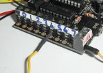
Note that when using terminal blocks it is necessary to ‘share’ the V2+ connector
with all output pins and to ‘share’ the V1+ connector with all inputs. Remember
that with the darlington driver output buffer the output devices are connected
between V2+ and the output (NOT output to 0V). Like wise the inputs are
connected between V1+ and the input.

Thank you
 

inglewoodpete

Senior Member
If you look at Appendix A of the CHI030a Datasheet (Page 7), you will see the circuit diagram of the CHI030a board.

You have the option of using of using two different power supplies to run the board by excluding the R9/Link between the supplies. If you do this, you will see that the common +ve bus on each side of the circuit will be connected to the different power sources. So, if you connect a 12 volt supply to the right-hand (output) side of the board (V2), then the right-hand common bus will have a potential of 12v, not 4.5 or 5 volts like the input (V1) side.

Of course, always use a 3 to 5v supply for the PICAXE and input side of the board (V1).
 

Tony P

Member
It states the following:

"Note that when using terminal blocks..."

Why should this make a difference? Surely using terminal blocks or soldering directly should make no difference?
 

Technical

Technical Support
Staff member
It states the following:

"Note that when using terminal blocks..."

Why should this make a difference? Surely using terminal blocks or soldering directly should make no difference?
When soldering wires you have 'pairs' of pads, so can simply use one pair per connection.
As Ec states, when you use terminal blocks it is not so easy to use the outer V+ holes of each pair. So most people share one V+ terminal block pin instead.
 
Top