Planning to control the brightness of a 1A LED from Off-1000mA using a hall effect sensor detecting the proximity of a magnet, running off a single 2.8-4.2v Li-Ion cell.
Originally I planned to use the LTC3454 driver, for which I could easily use a DAC controlled by the picaxe to manipulate the output.
Datasheet:
http://cds.linear.com/docs/Datasheet/3454fa.pdf
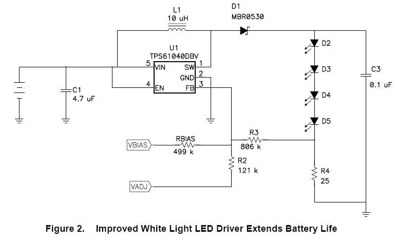
I then came across the TPS63000 by TI, while the LTC3454 can only manage 85% efficiency, or maybe 87% with 2 added diodes, where size is a concern, I decided I would try to use the TI product which can achieve well over 90% efficiency and uses a smaller inductor. Unlike the LTC3454 which is an LED specific constant current driver, the TPS63000, is a DC/DC voltage regulator which would need modification to work in a constant current mode.
TPS63000 Datasheet:
http://focus.ti.com/lit/ds/symlink/tps63000.pdf
I found some other TI literature on using a voltage bias technique to raise voltage on the feedback pin to lower power consumption across the current sensing resistor needed to run the TPS in a constant current mode.
http://focus.ti.com/lit/ug/slva268/slva268.pdf
Using a 2.5V voltage reference with a voltage divider to inject voltage into the FB pin allows the use of a smaller current sensing resistor.
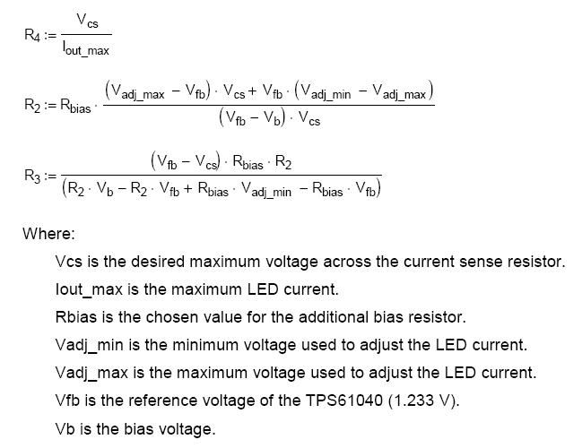
I found more TI literature about the voltage bias technique that has a formula for calculating these values.
http://focus.ti.com/lit/an/slva211/slva211.pdf
R8 = R6 [(Vf / Vref – Vcs) -1]
R8 = 248199
Vf = 3.5V
Vref = 0.5V
Vcs = 0.239V (value from the graph, using the 0.23 given value doesn’t equate)
R6 = 20K
Where Vref is the feedback reference voltage on the chip, and Vcs is the desired voltage across the current sense resistor.
Schematic for my Setup:
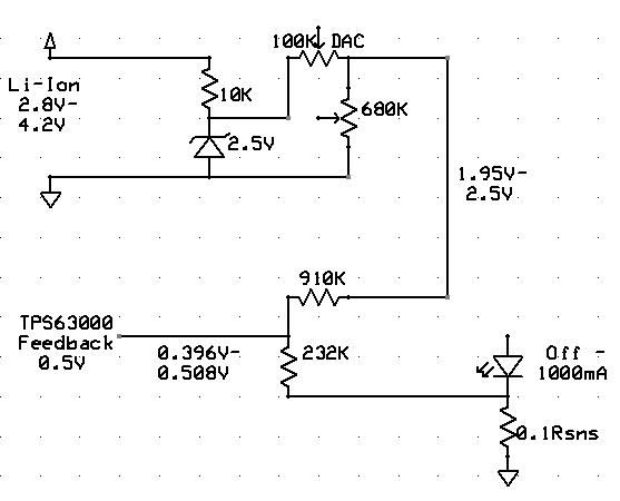
Using this formula, which is just a voltage divider formula, I get:
Vf = 1.95V - 2.5V
Vref = 0.5V
Vcs = 0V - 0.104V
“R6” = 232K
So,
“R8” = 910K
When The DAC is adjusted I get from 1.95V - 2.5V going into the second voltage divider, which then lowers this to a 0.396V - 0.508V signal for the biasing of the FB pin which gives from off, to just over 1000mA output using a 0.1Rsns current sense resistor.
Ideally I would have 0.4V - 0.5V going to the FB pin, but I’m giving myself some leeway on either side to take tolerances into account. The output minimum and maximum can then be set by the DAC.
The 680K pot is to adjust for the 20% tolerance in the 100K DAC.
For 1.95V - 2.5V output when DAC is adjusted,
If DAC = 100K then Pot = 345345R
If DAC = 120K then Pot = 425454R
If DAC = 80K then Pot = 283636R
The reason I’m doing it this way, is so I can use the 1.95V - 2.5V signal to feed the biasing voltage divider of multiple LED drivers to control their brightness.
I’m using 0.1% 910K and 232K resistors to try and keep the output of each driver as close as possible to each other, there is also the variance in the FB pin voltage of 0.495V - 0.505V, which can be accounted for then I set the high and low points of the DAC in the code to achieve (hopefully as low as) 20mA – 1000mA. I’m hoping the chips coming from the same batch will have a similar FB voltage to each other, so the output is well matched among drivers and I can lower the output to around 20mA without noticeable brightness difference between them. If it’s not possible, then maybe I will try to use current dimming down to 200mA or so and then PWM from there to lower output further.
There are some other documents from TI with other formulas using voltage biasing and voltage injection dimming here:
http://focus.ti.com/lit/an/slea004/slea004.pdf
http://focus.ti.com/lit/ug/slvu068/slvu068.pdf
Math isn’t my strongest point, and I couldn’t get the formulas in either document to equate with the given values, I suppose I’m doing something wrong with my rusty algebra. The values in these documents don’t work though, with the other method I used for determining the resistor values for the voltage divider, even though slea004 states that the injected voltage and the voltage across the current sensing resistor must add up to the FB pin voltage, which is what I’ve done in my case, so I’m not really too sure what’s going on with these docs, haven’t quite figured that out yet, I’m just hoping it’s going to work the way I have it planned.
It seems if I do figure out these docs, rather than having a voltage divider requiring a pot to tune for the tolerance of the DAC to inject 1.95V - 2.5V, I could just inject 0V - 2.5V through a resistor using the DAC alone as a voltage divider, and do away with the pot.
Just thought I would put this all into words as it helps me organize my thoughts, and if anyone sees any big mistake I’m about to make, please me let me know, I’ll be ordering the parts soon.
Originally I planned to use the LTC3454 driver, for which I could easily use a DAC controlled by the picaxe to manipulate the output.
Datasheet:
http://cds.linear.com/docs/Datasheet/3454fa.pdf
I then came across the TPS63000 by TI, while the LTC3454 can only manage 85% efficiency, or maybe 87% with 2 added diodes, where size is a concern, I decided I would try to use the TI product which can achieve well over 90% efficiency and uses a smaller inductor. Unlike the LTC3454 which is an LED specific constant current driver, the TPS63000, is a DC/DC voltage regulator which would need modification to work in a constant current mode.
TPS63000 Datasheet:
http://focus.ti.com/lit/ds/symlink/tps63000.pdf
I found some other TI literature on using a voltage bias technique to raise voltage on the feedback pin to lower power consumption across the current sensing resistor needed to run the TPS in a constant current mode.
http://focus.ti.com/lit/ug/slva268/slva268.pdf
Using a 2.5V voltage reference with a voltage divider to inject voltage into the FB pin allows the use of a smaller current sensing resistor.
I found more TI literature about the voltage bias technique that has a formula for calculating these values.
http://focus.ti.com/lit/an/slva211/slva211.pdf
R8 = R6 [(Vf / Vref – Vcs) -1]
R8 = 248199
Vf = 3.5V
Vref = 0.5V
Vcs = 0.239V (value from the graph, using the 0.23 given value doesn’t equate)
R6 = 20K
Where Vref is the feedback reference voltage on the chip, and Vcs is the desired voltage across the current sense resistor.
Schematic for my Setup:
Using this formula, which is just a voltage divider formula, I get:
Vf = 1.95V - 2.5V
Vref = 0.5V
Vcs = 0V - 0.104V
“R6” = 232K
So,
“R8” = 910K
When The DAC is adjusted I get from 1.95V - 2.5V going into the second voltage divider, which then lowers this to a 0.396V - 0.508V signal for the biasing of the FB pin which gives from off, to just over 1000mA output using a 0.1Rsns current sense resistor.
Ideally I would have 0.4V - 0.5V going to the FB pin, but I’m giving myself some leeway on either side to take tolerances into account. The output minimum and maximum can then be set by the DAC.
The 680K pot is to adjust for the 20% tolerance in the 100K DAC.
For 1.95V - 2.5V output when DAC is adjusted,
If DAC = 100K then Pot = 345345R
If DAC = 120K then Pot = 425454R
If DAC = 80K then Pot = 283636R
The reason I’m doing it this way, is so I can use the 1.95V - 2.5V signal to feed the biasing voltage divider of multiple LED drivers to control their brightness.
I’m using 0.1% 910K and 232K resistors to try and keep the output of each driver as close as possible to each other, there is also the variance in the FB pin voltage of 0.495V - 0.505V, which can be accounted for then I set the high and low points of the DAC in the code to achieve (hopefully as low as) 20mA – 1000mA. I’m hoping the chips coming from the same batch will have a similar FB voltage to each other, so the output is well matched among drivers and I can lower the output to around 20mA without noticeable brightness difference between them. If it’s not possible, then maybe I will try to use current dimming down to 200mA or so and then PWM from there to lower output further.
There are some other documents from TI with other formulas using voltage biasing and voltage injection dimming here:
http://focus.ti.com/lit/an/slea004/slea004.pdf
http://focus.ti.com/lit/ug/slvu068/slvu068.pdf
Math isn’t my strongest point, and I couldn’t get the formulas in either document to equate with the given values, I suppose I’m doing something wrong with my rusty algebra. The values in these documents don’t work though, with the other method I used for determining the resistor values for the voltage divider, even though slea004 states that the injected voltage and the voltage across the current sensing resistor must add up to the FB pin voltage, which is what I’ve done in my case, so I’m not really too sure what’s going on with these docs, haven’t quite figured that out yet, I’m just hoping it’s going to work the way I have it planned.
It seems if I do figure out these docs, rather than having a voltage divider requiring a pot to tune for the tolerance of the DAC to inject 1.95V - 2.5V, I could just inject 0V - 2.5V through a resistor using the DAC alone as a voltage divider, and do away with the pot.
Just thought I would put this all into words as it helps me organize my thoughts, and if anyone sees any big mistake I’m about to make, please me let me know, I’ll be ordering the parts soon.