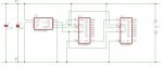
This circuit uses two serial to parallel chips (74HC595) to expand the number of outputs. It takes 3 outputs and converts to 16 outputs, and is also expandable to any arbitrary number and will work on any picaxe. This circuit is useful for driving two seven-segment displays or any task where lots of outputs are needed. The QH output (pin 9) can be cascaded to pin 14 of the next chip. All the bits are fed out one at a time and then the data is latched to the output pins.
' dual HC595 routine - 16 digital outputs
' uses any picaxe - pins 0,1,2
' pin0= latch clock HC595 leg 12 - low to high transition latches the data
' pin1 = serial data out = HC595 leg 14
' pin2= shift clock = HC595 leg 11 - low to high tranition stores the serial data out
' HC595 goes from left one to right one. Left one is MSB = the left 8 bits of the w0 word
' HC595 leg 11s in parallel
' HC595 leg 12s in parallel
' HC595 leg 9 of left one is the SQH bit output and goes into leg 14 of the right HC595
' HC595 reset legs 10 are both high
' HC595 output enable legs 13 are both low
main:w0=%1000000010000001
gosub senddatatolatch
pause 1000
w0=%0000000000000000
gosub senddatatolatch
pause 1000
goto main
senddatatolatch:' sends data in w0, uses register b2 and b3
' note QA is MSB and QH is LSB (binary number reads down) feed in LSB first
low 2' low leg 11
low 0' low leg 12
low 1' low leg 14
for b2=1 to 16
'*****b3=w0 and %00000001' check rightmost bit status
'*****if b3=0 then See post #5 - 2 lines replaced with one line
if bit0=0 then
low 1' serial data
else
high 1' serial data
endif
high 2' low to high transition stores the serial data
low 2
w0=w0/2' shift bits to right one place
next
high 0' latch the data and send it out - HC595 leg 12
low 0
return
Attachments
-
 46.6 KB Views: 619
Last edited:
")