Description and code/circuit options further revised and posted starting at #5
This post publishes the work discussed in the thread;
http://www.picaxeforum.co.uk/showthread.php?t=10039
NOTE:- Revised description, code, and circuit published 7 August 2008 (BCJ). and incorporates additional contributions from Hippy and further refinement/testing. Updates shown in italics.
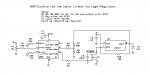
The concept is to use an 08M to control the resistance of a MOSFET and use this MOSFET to replace the adjustment Potentiometer (typically 'R2') in the standard circuits for LM317 type adjustable 3 terminal regulators.
A potentiometer is still used to instruct the 08M what output is required. Alternatively the ADC Value - (SetVar, or Target in the MKII code) could be delivered by any mechanism of your choosing.
Why bother?
Program control via the 08M does provide some advantages. As stated by Hippy:- "I like the idea of PICAXE control to (1) smooth out the pot and stop 'track skip', (2) allow arbitrary pots to be used ( even log / anti-log ), (3) the ability to set voltage limits and (4) the ability to set voltage ranges. It's particularly useful to prevent the output going above a certain voltage and stops accidentally connecting high voltages to low voltage circuits when the pot gets knocked."
Wilf_nv published the original circuit
Wapo54001 proposed Wilf's circuit as a possible solution.
Many contributed and, Wapo and BCJ tested different systems.
Debate raged on the best place to pick up the feedback information ~ from the Regulator Vout, or from the Adj Circuit itself.
Vout would appear to be the most logical place as this avoids any issues of the feed back network interacting with the MOSFET variable resistor. In practice, both seem to work well.
The details published below show the Vout sensing circuit and program as tested for 10V output.
The MOSFET seems not to be critical. (Note:- Some "ringing" issues under load have been found with the VN2222L and Vout sensing). The circuit as published was tested using a Bench supply delivering 5V for the PICAXE and 13V Vin for the Regulator for a 1.25 to 10V output.
The regulator tested was an LM317T from ST
Load was applied via resistors.
An LED is required across the Output to provide the required minimum current of 3.5 to 10mA if not using a dummy load else the regulator is unstable.
Tests were carried with out no capacitors on the LM317T.
Minimum Vout for an LM317T is 1.2V
Maximum Output is Vin - 3V, Maximum Vin is 40V
The Data sheet graphs show that once the differential (Vin - Vout) exceeds 12.5V, current capacity drops off rapidly. However the tabulated electrical characteristics show the rated 1.5A for an LM317T is available at Vin - Vout of 15V!
This suggests that for a circuit starting at the minimum 1.2V, 10.8V is the maximum Vout before current reduction starts. (15 - 3 - 1.2 = 10.8V)
The circuit below was tested with two quite different logic level MOSFETS, a Vishay VN2222L and an IRL520N Hexfet. It was also tested with a power (not Logic level) MOSFET MTP3055E TMos 'StripFET'.
All performed admirably with no change to circuit or program although the response varied with the best from the VN2222L and the worst from the MTP3055E. Note some issues found with CRO and the VN2222L
The alternate circuit (obtaining feedback from the adj circuit) was also tested with the VN2222L solely by relocating the wire from the top end of the divider from Vout to Adj.
Please note:-
1. Should the LM317T be powered while the 08M is not, Vout is uncontrolled and floats high. Ensure that the 08M is powered and running first (gate voltage will be 0V) and then turn Vin on, or, turn both on together - i.e derive 08M 5V supply from whatever turns on Vin.
2. Some fine tuning of the Gate Charge Capacitor may be required to obtain smooth and fast tracking of Vout to Adjustment Pot movement depending on MOSFET characteristics. Have had best results with IRL520N and 0.15uF
3. Should you wish to implement this circuit, please read the full thread referenced above, and study all the data sheets.
This post publishes the work discussed in the thread;
http://www.picaxeforum.co.uk/showthread.php?t=10039
NOTE:- Revised description, code, and circuit published 7 August 2008 (BCJ). and incorporates additional contributions from Hippy and further refinement/testing. Updates shown in italics.
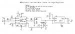
The concept is to use an 08M to control the resistance of a MOSFET and use this MOSFET to replace the adjustment Potentiometer (typically 'R2') in the standard circuits for LM317 type adjustable 3 terminal regulators.
A potentiometer is still used to instruct the 08M what output is required. Alternatively the ADC Value - (SetVar, or Target in the MKII code) could be delivered by any mechanism of your choosing.
Why bother?
Program control via the 08M does provide some advantages. As stated by Hippy:- "I like the idea of PICAXE control to (1) smooth out the pot and stop 'track skip', (2) allow arbitrary pots to be used ( even log / anti-log ), (3) the ability to set voltage limits and (4) the ability to set voltage ranges. It's particularly useful to prevent the output going above a certain voltage and stops accidentally connecting high voltages to low voltage circuits when the pot gets knocked."
Wilf_nv published the original circuit
Wapo54001 proposed Wilf's circuit as a possible solution.
Many contributed and, Wapo and BCJ tested different systems.
Debate raged on the best place to pick up the feedback information ~ from the Regulator Vout, or from the Adj Circuit itself.
Vout would appear to be the most logical place as this avoids any issues of the feed back network interacting with the MOSFET variable resistor. In practice, both seem to work well.
The details published below show the Vout sensing circuit and program as tested for 10V output.
The MOSFET seems not to be critical. (Note:- Some "ringing" issues under load have been found with the VN2222L and Vout sensing). The circuit as published was tested using a Bench supply delivering 5V for the PICAXE and 13V Vin for the Regulator for a 1.25 to 10V output.
The regulator tested was an LM317T from ST
Load was applied via resistors.
An LED is required across the Output to provide the required minimum current of 3.5 to 10mA if not using a dummy load else the regulator is unstable.
Tests were carried with out no capacitors on the LM317T.
Minimum Vout for an LM317T is 1.2V
Maximum Output is Vin - 3V, Maximum Vin is 40V
The Data sheet graphs show that once the differential (Vin - Vout) exceeds 12.5V, current capacity drops off rapidly. However the tabulated electrical characteristics show the rated 1.5A for an LM317T is available at Vin - Vout of 15V!
This suggests that for a circuit starting at the minimum 1.2V, 10.8V is the maximum Vout before current reduction starts. (15 - 3 - 1.2 = 10.8V)
The circuit below was tested with two quite different logic level MOSFETS, a Vishay VN2222L and an IRL520N Hexfet. It was also tested with a power (not Logic level) MOSFET MTP3055E TMos 'StripFET'.
All performed admirably with no change to circuit or program although the response varied with the best from the VN2222L and the worst from the MTP3055E. Note some issues found with CRO and the VN2222L
The alternate circuit (obtaining feedback from the adj circuit) was also tested with the VN2222L solely by relocating the wire from the top end of the divider from Vout to Adj.
Please note:-
1. Should the LM317T be powered while the 08M is not, Vout is uncontrolled and floats high. Ensure that the 08M is powered and running first (gate voltage will be 0V) and then turn Vin on, or, turn both on together - i.e derive 08M 5V supply from whatever turns on Vin.
2. Some fine tuning of the Gate Charge Capacitor may be required to obtain smooth and fast tracking of Vout to Adjustment Pot movement depending on MOSFET characteristics. Have had best results with IRL520N and 0.15uF
3. Should you wish to implement this circuit, please read the full thread referenced above, and study all the data sheets.
Last edited: