Hi,
There might be quite a lot of useful ideas in the Teletext system; the memory and processing limitations in those days may be rather similar to PICaxe now. It also had "block graphics" characters, dividing each cell into 6 rectangles (i.e. 2 x 3, coded into 64 characters) and had the option to display a blank line between these sub-blocks, so that the cell boundaries didn't predominate. The "character rounding" algorithm was applied to interlaced (TV) displays, but interlace refreshes at only 25 Hz (30 Hz USA) so individual pixels can suffer "interlace twitter" and some people preferred to disable interlace to give a more "pixellated", but stable display. Of course Teletext also supported "double height" characters and I plan to post my first trial algorithm in the Code Snippets section soon.
I don't want to hijack this thread, but as the OP asked.....
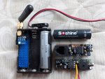
"projects .... the size of an AA cell".....
It would be interesting to see a photo of one if you have one to hand and it's not too much trouble.
Photo of a few samples attached; there are basically two power supply styles: (1) The end tags receive the full supply voltage from other (AA) cells in the battery pack and the normal power connector terminals / wires can optionally go to an on/off switch. Note that the "tip" (screw) connection to the board is actually earth and the "body" receives the supply voltage. (2) Alternatively, the end terminals can be connected by a low resistance (a few ohms) to allow the PICaxe to monitor the current and the full supply is obtained on a "fly lead", typically terminated with solder tag which can slide in at the top battery terminal. The version with a "sounder" has a second wire to monitor the balance between two cells and a transistor (2N7000) to disconnect the load.
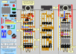
However, I can go further: a few years ago, Westaust55 had a few "spare weeks" and we cooperated to update his "Pebble" application to accommodate some of my "pseudo PCB" construction methods. These often use Veroboard (copper-clad stripboard) but can also use naked "perf.board" or prototyping boards with individual (double-sided) pads, linked by Plated Through Holes. My very small Veroboards need numerous track-cuts and there can be problems with the copper lifting (during soldering), so the PTH boards are interesting. But I normally design in Veroboard form, partly because that's what Pebble supports, and also it can be very tedious creating all interconnections at only 0.1 inch (2.5mm) at a time.
The construction method that I use is to fold over the through-hole leads on the underside of the board, to imitate PCB tracks. Longer spans and top-side links for a "double-sided" capability use "BTC" (Bare Tinned Copper) wire with a gauge of around 24 swg. The additions to Pebble allow these links to be routed not only N, S , E and W but, also NE, SE, SW and NW and even some more distant "diagonal" paths. Additional component outlines include a "screw" to represent the positive terminal of an AA cell and an "upright" 3.5 mm Programming Socket which fits across the other end of the board to resist the pressure from the battery holder spring. This Programming Socket is one of the "floating" components (it isn't locked to the 0.1" grid) because it is one hole narrower than the PCB, so can fit with its pins between the copper tracks (also giving better adhesion).
For acceptable design flexibility, the PCB needs to be 6 holes wide (i.e. 4 holes for the DIP socket and typically a supply and ground rail along the sides. That would be a width of 15.25 mm which is greater than the nominal 14 mm diameter of an AA cell, but the "gap" between copper tracks is not needed and the edge tracks can be cut (or filed) back slightly without affecting their function as "rails". In an extreme, the outer tracks could be "broken" along the line of holes, but this is not recommended because it is so much more difficult to locate the component leads during soldering. Of course the cross section of an AA cell is circular but the assembled boards normally have a "square" cross section, so cannot be used in the (few) battery compartments that have a curved contour (or even "end -feed") to accept the cells. But the majority of battery holders have a simple box section, so the PCB can have dimensions of about 14 x 50 mm and still fit near the base of the compartment.
There are a few "design rules": The majority of through-hole components will be mounted vertically; normal MR/CR25 ("quarter watt") resistors (the 25 actually refers to their diameter in tenths of a mm) are intended for 10 mm hole spacing (cf. height) but in practice can be bent to 7.5 mm height / hole spacing. We only need 6.3 volt (electrolytic) capacitors so size shouldn't be much of a problem, but it may be necessary to choose a manufacturer / range with a maximum height of 6 or 8 mm. Also, I try to mount components on the middle 4 tacks and only allow wires / leads to terminate on the two (supply / ground) narrower side strips and sometimes components (and certainly links) may need to be located under the ICs. Both Pebble's 0.1 and 0.2" pitch resistors will be mounted vertically in practice, and it isn't possible to show 0.15" (diagonal holes) or the "handed" nature of vertical resistors (i.e. on which side the body lies relative to the wire), so some interpretation may be required.
PEBBLE does permit a 6 x 20 holes PCB to be designed directly, but it is difficult to show all details of such compact designs. Therefore I normally work with a layout of about 24 x 20 holes "masked" into three strips of 6 x 20. These strips can be used to compare "trial" layouts, but ultimately I usually show the (reversed) underside (solder side) layout in the middle, particularly to indicate the exact positions of "spot face" or track cuts. The "CUT" symbol was intended to show tracks broken by two parallel knife (scalpel) cuts, between a pair of holes, with the intervening copper "popped off" using a hot soldering iron. It's a good way to prepare fully-designed layouts, but cutting tracks once some solder has been applied is difficult. So now, I generally show spot face cuts (made with a twist drill or custom cutter) and find the CUT symbol more useful in the preliminary design stage, particularly in an "overview" of the main parts of the design in the first strip. The final strip may show just the "topside tracks", or a "final view" (e.g. with ICs installed) depending on the nature of the design.
Here is my first trial for an AA OLED display board, which includes a software-controlled HSERIN inverter (when C.4 is low) that can also switch a LED (OFF when C.4 is floating or low). It includes provision for a DIP8 I2C EEPROM which might be used as a "scratchpad" or for temporary or permanent storage of character shapes, or for ASCII text or graphics, etc. The 128 x 32 OLED is rather longer than the 128 x 64 display so the header pins need to be almost at the end of the PCB. That has required a few "cheats": The screw (battery tip) is only allocated one hole (~2.5mm) whilst I normally allow for a 6 mm (1/4") x M3 pan head. However, the row used by the LED and resistor could be omitted and the two I2C bus pullup resistors might be replaced by the internal Weak Pullups (since the "bus" is literally only 1 or 2 cms long, with no earth plane). Another "cheat" is that the four pins along one side of the EEPROM (GND and A0 - A2) are assumed to be all earthed together (which they can be) on the top side of the board, with three (socket) pins cut off so that the solder-side tracks can link the PICaxe and OLED. This is easier with my preferred "turned pin" style of socket (or header strip) than the fully moulded type. Unfortunately, the 128 x 64 pixels OLED effectively has its pins in the reverse sequence so may require a different arrangement, probably with the EEPROM rotated by 180 degrees (which would then make it the same orientation as the PICaxe).
There's a lot more that could be said, but I think better saved for a dedicated thread, sometime.
")
Cheers, Alan.