PhilHornby
Senior Member
What's a Quick Charge Trigger Board, I hear you say ")
The Qualcomm Quick Charge protocol is implemented by a variety of 'USB' Chargers and (more interestingly, perhaps) Power Banks. They are intended for 'quickly' charging Mobile phones and Tablets. This is achieved by increasing the voltage from the default 5V, to 9V, 12V or maybe even 20V. The idea seems to be, that by supplying the same power at a higher voltage (and proportionately lower current), it is easier for the phone's charging circuits and cabling to cope with. I have no idea how much benefit this actually conveys, but I'm more than willing to exploit these devices for other purposes
There are other, equally proprietary methods that exist to achieve the same goal - but the Qualcomm Q.C. 2.0 and 3.0 protocols are documented around the web. Dedicated ICs exist to implement the protocols, but it turns out that they are actually extremely simple.
All the technical detail required to implement the protocol can actually be found on Page 9, of this datasheet: https://www.onsemi.com/pub/Collateral/NCP4371-D.PDF.
(These are also worth perusing: CHY100 datasheet, FAN6290QF datasheet and the TPS61088 datasheet)
Here is some of the information in visual form:
(The guy sounds like Kimi Raikkonen to me )
There is also a wealth of information here: http://blog.deconinck.info/post/2017/08/09/Turning-a-Quick-Charge-3.0-charger-into-a-variable-voltage-power-supply
(For some reason, this chap chose a slow, large, expensive Picaxe competitor )
In a nutshell: A 'low' voltage (>0.6V and <2V) is applied to D+, for more than 1.25S. This voltage will (probably) be reflected onto the D- line, as per the Battery Charging V1.2 Specifications. A Qualcomm Quick Charge compatible device, will respond to this signal, by dropping D- to GND potential, at which point, its Voltage o/p can be controlled by setting the correct combinations of voltage on D+ and D-. This is Q.C. 2.0 and it exists in two flavours - the first "A" allows a voltage upto 12V and "B" allows 20V. These signals are quite 'analogue': >0.325V or >2V being commonly quoted for the two levels.
One combination of signals was spare and was used to implement Q.C. 3.0. By pulsing these signals, it is now possible to step up or down 200mV at a time (again to either 12V or 20V)
I present here three small programs, two of which share hardware and a third which requires a small modification.
The programs are as follows:-
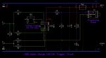
Circuit for Program 3
(Ooops! I think R8 has morphed from 100K to 10K in this rendition)
The Qualcomm Quick Charge protocol is implemented by a variety of 'USB' Chargers and (more interestingly, perhaps) Power Banks. They are intended for 'quickly' charging Mobile phones and Tablets. This is achieved by increasing the voltage from the default 5V, to 9V, 12V or maybe even 20V. The idea seems to be, that by supplying the same power at a higher voltage (and proportionately lower current), it is easier for the phone's charging circuits and cabling to cope with. I have no idea how much benefit this actually conveys, but I'm more than willing to exploit these devices for other purposes
There are other, equally proprietary methods that exist to achieve the same goal - but the Qualcomm Q.C. 2.0 and 3.0 protocols are documented around the web. Dedicated ICs exist to implement the protocols, but it turns out that they are actually extremely simple.
All the technical detail required to implement the protocol can actually be found on Page 9, of this datasheet: https://www.onsemi.com/pub/Collateral/NCP4371-D.PDF.
(These are also worth perusing: CHY100 datasheet, FAN6290QF datasheet and the TPS61088 datasheet)
Here is some of the information in visual form:
)There is also a wealth of information here: http://blog.deconinck.info/post/2017/08/09/Turning-a-Quick-Charge-3.0-charger-into-a-variable-voltage-power-supply
(For some reason, this chap chose a slow, large, expensive Picaxe competitor
)In a nutshell: A 'low' voltage (>0.6V and <2V) is applied to D+, for more than 1.25S. This voltage will (probably) be reflected onto the D- line, as per the Battery Charging V1.2 Specifications. A Qualcomm Quick Charge compatible device, will respond to this signal, by dropping D- to GND potential, at which point, its Voltage o/p can be controlled by setting the correct combinations of voltage on D+ and D-. This is Q.C. 2.0 and it exists in two flavours - the first "A" allows a voltage upto 12V and "B" allows 20V. These signals are quite 'analogue': >0.325V or >2V being commonly quoted for the two levels.
One combination of signals was spare and was used to implement Q.C. 3.0. By pulsing these signals, it is now possible to step up or down 200mV at a time (again to either 12V or 20V)
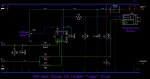
I present here three small programs, two of which share hardware and a third which requires a small modification.
The programs are as follows:-
- QC_Preset_Voltage: The required voltage is hard-coded in the program source; it cannot be varied at run time. The fixed Q.C. 2.0 voltages can be used, or the more granular QC 3.0 offerings. The switch shown in the schematic is not required - though I was using it as RESET switch, for debugging purposes.
- QC2_Toggleable_Voltage: This uses the push-to-make switch to toggle between the available voltages. The last selection is stored in EEPROM and reselected at the next power-up. It can only select the fixed Q.C. 2.0 voltages. If the switch is depressed at boot time, the Voltage is guaranteed to be reset to 5V.
- QC3_Variable: By adding a potentiometer, the output voltage can be selected in 200mV steps between 5V and 12V. (If you are lucky enough to find a "B" version of a charger or Power Bank, you would need to rework the code to support it. As well as the aforementioned 20V output, there is also rumour that the voltage can be lowered below 5V (to 3.6V). I do not possess such a device to try it. Adding the potentiometer, meant that the simple resistor network that drives the D- line, had to be replaced by a resistor/capacitor network - fed from PWM signal.
Circuit for Program 3
(Ooops! I think R8 has morphed from 100K to 10K in this rendition)
Attachments
-
6 KB Views: 3
-
6.9 KB Views: 3
-
6.6 KB Views: 2
Last edited: