PWM for Transistor Switching

Sodapep

Member
Hello!

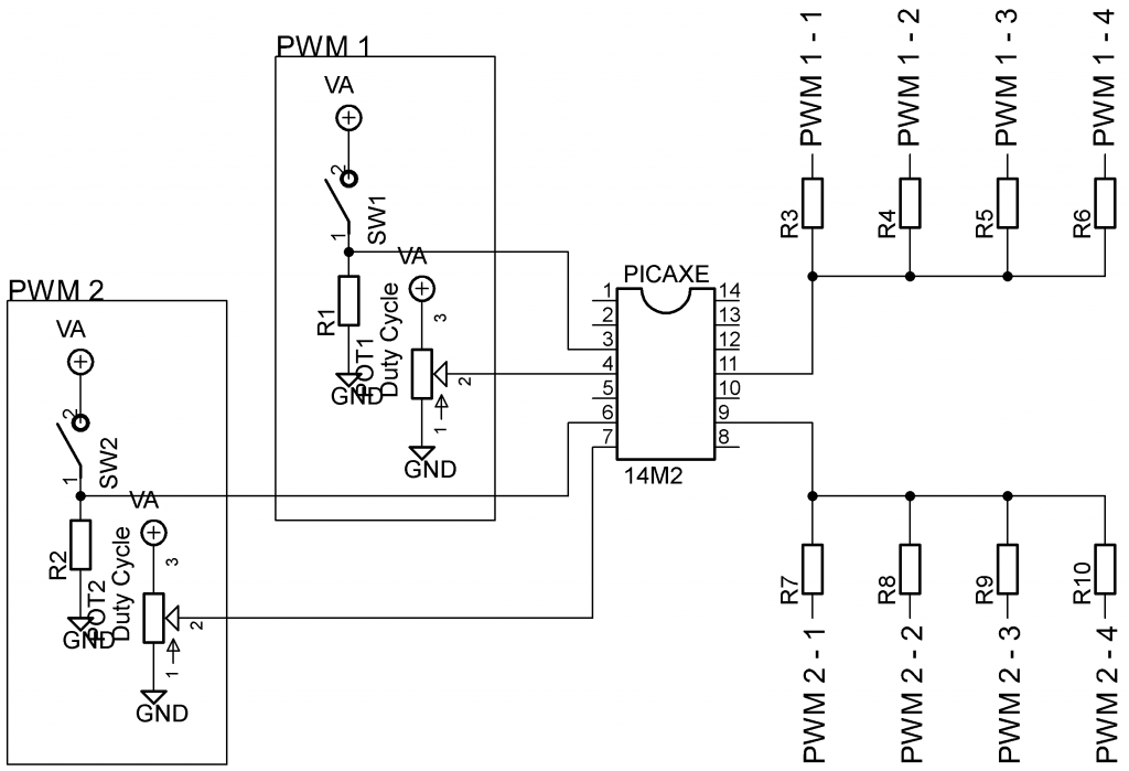
I'm working on an idea currently (code to come later, if the idea fleshs out well) for using the PWM out of the PICAXE to the base of a BC560 (or similar) transistors acting as a current controlled resistors. There are many levels of things I don't understand, so I'll start with the basic idea of the project.

Eight transistors in total are being used as the current controlled resistors. In normal operation of the device, four of them will be held high in saturation for the least resistance and the other four will be held low for infinite (I guess? or at least very large) resistance by the PWM. There are four interfaces for a user - two switches and two potentiometers. When one button is pushed and held, the transistors held high will begin to decrease in voltage as the PWM slows at a rate that is defined by the definition of the pot. The other pot and switch act in the same way, but it increase the transistor up to saturation. Upon release of a button, the PWM goes back to its normal rate at a speed based off of the speed at which it changes (most likely faster, but related to the initial speed). Both buttons will not be expected to operate at the same time, but both PWM signals need to be constantly running.

As I said, there are many levels I don't understand. The PICAXE can read the two buttons inputs on two pins by applying 5V when pushed. Two seperate pins can read the potentiometer value, but I don't know how to apply that to the rate of the PWM, if at all possible? The PWM should probably also be constrained between just below the turn on current/voltage of the transistor (so their isn't dead space at the bottom of the PWM wave) and the max 5V. I've seen projects where LED's are set to pulse/dim with the PWM, but I'm not sure how to drag that out into this project.

Some other confusions: is it possible to use a current mirror and power all four transistors off of one pin of the PICAXE? That way an 14M2 can be used instead of something much larger with 8pwm outputs (I believe the 08M2 only has 1 pwm output?). Is it even possible to have two different PWM's coming from the same chip, or will I need to use two 08M2's? Does anyone have better ideas :D

Thank you for lending your amazing brain powers.
 

Paix

Senior Member
Sorry that I don't have much to contribute, but I think that you will find that it isn't the PWM rate that will need to be varied, but the duty cycle. You will choose a suitable PWM rate/frequency that suits and the mark/space ratio will determine the effective average voltage level, perhaps across an integrating/smoothing capacitor.
 

Sodapep

Member
Right you are! I was inappropriatly calling the difference in time 'on' and 'off' the rate when it is the duty cycle. The rate would be the set crystal in the PICAXE I suppose. Thanks Paix! Making progress.
 

Paix

Senior Member
I had a feeling that it was just in the nomenclature, but best to have checked that you weren't barking up a wrong tree.

Transistor = Transfer Resistor , , , definitely current controlled.

@Sodapep, is it possible to produce a clear drawing that would give a clearer idea of the layout you envisage. You mention two independent PWM signals, so you will be probably be talking about an 14M2, 18M2 chip or greater

Your text I find confuses me, but my interpretation is thus:

You wish to use BC560 (or similar) PNP transistors to as high level switches. Because ?
The default tends to be an NPN transistor or FET used as a low level switch, as it allows simple switching of +5V or voltages greater than the Picaxe supply voltage without undue complications.

You don't specify what your intended load is, but it sounds like lighting of some sort. Please let us know.

Eight channels
Two switches commanding ramp up/down
Two potentiometers controlling speed of change.

How are the channels to be grouped?
What is the relationship between channels or groups and both the switches and the pots?

This will give a better idea of exactly what you want. Best to make your points briefly with lots of white space to make it readily digestible by the average brain.
 

Sodapep

Member
That sounds mostly right! I guess I was a little too vague in the OP.

I'm working with a circuit that uses resistance between two pins to set a delay time. There is normally a 50 to 100k potentiometer in this feedback loop that reads the resistance and sets the delay time. I have successful (with a lot of help!) strapped a BC560 into this loop in series with the potentiometer with an LFO modulating the base of the transistor in order to vary the delay time by adding and subtracting resistance within the loop. There is a resistor paralelled with the collector and emitter as well. This modulates the resistance which modulates the delay time. The LFO can be set to subtle or extreme.

Adding onto this idea, I would like to have two operations. The first is attach another transistor in a similar fashion - in series with the other transistor and potentiometer - but rather than moduate the resistance, I'd like to have it be fully open until a button is pushed. When the button is pushed, the resistance of the transistor will begin to increase due to the decreasing amperes at it's base based on the time set by a potentiometer. This will cause the delay time to increase over time.

Second - have another transistor set up in parallel with the whole circuit described above. However, this will be fully closed, having little effect on the resistance within the loop. When the second button is pushed, the base of the transistor will be fed amperes at a rate based on the second potentiometer, decrease the resistance in the delay time loop, effectively causing the delay time to shorten.

Now that is the description of one loop - there are four of these :confused: There are two groups - one button and one pot for each. Each group contains four transistors of the same use - one group has all the transistors that increase in resistance and one group has all the transistors that decrease. Pushing one button will change the state of the four transistors at the same time within its buttonly jurisdiction.

I hope that made a bit more sense. I'll be able to draw a picture of the delay loop this evening if it didnt...
 

premelec

Senior Member
I'm not entirely following what you're thinking of but suggest that if you don't need fast adjustments you can use one pot with READADC value which is put in a _selected_ variable to control that channel and you can have 4 set PWMOUTs for instance from a 14M2 PICAXE... A circuit diagram would help as well as a simple statement of what the inputs and outputs are - together with block diagram.
 

Sodapep

Member
And now, the pictures you've all been waiting for!

First is a picture comparing how I currently have it set up on the left, then the idea setup on the right.


Currently the resistance within the loop of the IC is being varied by the interface pot, but also modulated by an LFO modulating the base of the transistor. There are x4 in the titles because there are four separate IC's within the device that this is occurring in. In the ideal setup, there are two more transistors added. One, attached to PWM 1, will be held open normally. When a switch is activated, the PWM 1's duty cycle will lower at a rate set by a potentiometer, effectively increasing the resistance in the loop. The second transistor, controlled by PWM 2, will be normally closed with PWM 2 below the turn on value of the transistor. When a different switch is activated, the PWM 2 duty cycle will rise at a rate dependent on another potentiometer, decreasing the resistance within the loop. Next picture - the interface set up.


Now, with the picaxe in play, there are two sets of controls, each consisting of a button and pot. One set of controls is for pwm 1, the other for 2. There are two pwm outputs happening simultaneously, going to each PWMx input on each of the four circuits. When a switch is engaged, all four transistors will experience the same shift in PWM. I hope I'm starting to make sense of this idea!
 

Paix

Senior Member
@Sodapep, you should be glad of the post that never actually made it . . . my vision was quite different from your diagram . . . I see now that the active diagrams are the large bottom one and the top right hand one one.

It occurs to me that with three transistors in a totem pole arrangement, that the Picaxe drive to those bases will have to be isolated somehow, as each base junction will to see something around 0.3V before it will begin conducting and so maybe opto couplers, such as 4N25 might be called for. That would certainly satisfy the Picaxe side of things and allow the for the level translation as all the transistor emitters are at different voltage levels, but the transistor bases may need to take some form of biasing from their individual collectors or emitters. Something for the 4N25 output transistor to switch, as I'm not sure if there is enough leakage from the PNP base to rely upon that alone.

This is more than a little out of my knowledge zone. Nice pictures, but what is the IC device that is being controlled? There has to be a voltage between the pins 3 and 4 and 3 has to be positive with regard to pin 4.

I still haven't really got a clue as to what is supposed to be happening. I get an impression of effective resistances ramping up and down upon command and a set level between times, but nothing more. The pot marked delay, can only be a delay if there is capacitance involved somewhere.

What sort of frequency is the LFO going to be running at and what sort of frequency for the pwm. The effective resistance will actually be quite a complex signal voltage, so where will the low pass integrator be to get rid of all the hf signal component from the pwm?

I have to be back up in a couple of hours, so I think I will go to bed now. I really don't know what it is that you wish me to understand and without knowing anything about the device, you are talking resistance and I'm thinking voltage/current control. I don't understand your rationale for using PNP transistors and have to wonder at their ultimate significance other than a desire to operate with negative logic?

Is it really just being artificially complicated, when a lot less hardware would perhaps do the job if we only knew what that actually was?
 

StigOfTheDump

Senior Member
I don't really understand what your circuit is for.

It appears that you are sending a PWM signal from the picaxe to your existing circuit, which then alters an incoming signal back into the picaxe.

Would there not be a mathematical solution with the button and pot in series being one input to the picaxe and your existing circuit being another?
 

Sodapep

Member
Yikes - seems like I'm not doing a great job at explaination! The over arching idea is to get resistance changes within the loop - the actual chip (PT2399) puts out a VCO through the loop which ends at the digital ground through the second pin. The resistance in this loop determines the actual signal delay time that the chip produces. The larger the resistance, the longer the delay time. I had originally planned to use vactrols in place of transistors, but they were expensive and had a lot of variability - if that help with understanding the idea any more. Basically I'm looking for a vactrol replacement.

Normally, there is a just a single resistance in this loop, the potentiometer. (In the schematic on the left) the transistor that is added acts as a variable resistance based on the LFO frequency. As the amperes wiggle around on the base, the transistor and it's parallel resistor give slight variations in the resistance read by the IC. This causes the delay time of the chip to warble around.

Now, rather than warbling, I'm trying to add two more transistors that operate under the same idea of variable resistance, but ramping rather than warbling (is that a word? wobbling maybe?). Back to the vactrol comparrison - the transistor with PWM 1 would have the LED at full brightness. When the PWM 1 switch was engaged, the brightness would dim at a rate set by the PWM 1 pot. In contrast, the PWM 2 would have the LED on full darkness (giving full LDR resistance). When PWM 2 switch is engaged, the LED would begin to increase in brightness at a rate determined by PWM 2 pot. Does that make any more sense?
 

JimPerry

Senior Member
Is this for a analog/digital audio synth/stomp box? Vactrols have a "warm" sound not easily replicated. :rolleyes:
 

Sodapep

Member
It is indeed for my modular synth setup.

The warm/roundness of the LDR isn't really needed in this case. I had been doing the modulation via a vactrol as well, but the transistor sounds just as good at all settings. I suppose if it is indeed too much of a mess to use transistors, I could go back to vactrols - but the inconsistencies and the min resistances are going to be problems.
 

Paix

Senior Member
@Stig. . ., at least if Sodapep was in Australia, we would know which direction to be digging in. :) I don't have answers, but seek the right question.


The biggest clue really is the device type PT2399 . . .Still not a clue as to the application, but Mr Google speaks my language just fine.

Mr Google, he says, “Ian, you have looked up this device several times a few months ago . . . it is a reverberation chip, or more accurately an analogue/digital delay line.”

A circuit source
A PT2399 datasheet
In your post #8 your 'network' is connected between pins 3 and 4 of either IC1 or IC2, which I believe is the PT2399 chip. Unfortunately these two pins are respectively Analogue ground and Digital ground . . . Hmmm. The evidence seems to suggest that we are looking to tailor an effective resistive response, in the approximate range of 10k to 50k between the Digital ground pin 4 and the VCO control input, pin 6. *** Voltage Controlled Oscillator **
There are x4 in the titles because there are four separate IC's within the device that this is occurring in
The device was assumed to be what we now believe to be the PT2399, but it is the actual item of equipment . . .
= =
The real question is, “How can we dynamically control the VCO in a PT2399 employing a Picaxe chip and a suitable program?”
= =
Question, what is the range of the voltage on pin 6 in normal operation, when twiddling a 50k potentiometer? What is the voltage on pin 6 if it is left open (disconnected from any resistor)?

Open question, how can we influence the voltage appearing on pin 6 in order to gain control of the VCO other than by sticking in a resistor?

Thoughts: the anticipated use of the PT2399 chip, the external control resistor must form part of a voltage divider network. By a process of substitution of various resistor values and voltage measurements, the effective value of the unknown resistor can be ascertained, but is unlikely to be of much interest.

If a controlled voltage is injected into pin 6, then it will control the VCO output frequency.

Question, on pin 6, does a low resistance = low frequency, or low resistance = high frequency?

Single PT2399 implementation: A 15kHz to 20kHz pwm signal from the Picaxe is used to control the voltage on pin 6 as shown in the diagram.

C1 is an AC coupling capacitor
D1 is a signal detector
R1, C2 is an integrator filtering out the hf AC, leaving the rectified DC level
R2 is a passably low resistance to set the lower voltage limit
nothing is guaranteed.


Code:
pwm in ---C1--D1--R1---+---+--pin6
                       |   |
                       R2  C2
                       |   |
                      Gnd Gnd
I think that we are getting there now, how does this generally sound to you? I believe that there are four PT2399 in your equipment? What is that equipment please and what is the final application, guitar reverb?

Footnote:
My considered use for the PT2399 was to allow a transmitter to be keyed from a data signal, but delay the signal for a couple of mS to prevent the clipping of the first data symbols.
In the end I determined that the degree of distortion for the delay I desired was unacceptable.
 

JimPerry

Senior Member
It is indeed for my modular synth setup.

The warm/roundness of the LDR isn't really needed in this case. I had been doing the modulation via a vactrol as well, but the transistor sounds just as good at all settings. I suppose if it is indeed too much of a mess to use transistors, I could go back to vactrols - but the inconsistencies and the min resistances are going to be problems.
You might want to try experimenting with cheap opto-isolators (4N25 http://www.ebay.com/itm/New10x-4N25-OPTOISOLATOR-PHOTO-TRANSISTOR-SEMICONDUCTOR-/320524210306?pt=LH_DefaultDomain_0&hash=item4aa0bb5082) - drive the LED with PWM and Bob's a male relative? :confused:
 

premelec

Senior Member
I agree w/ JimPerry - an opto might work for you but not a photo bipolar transistor but photo FET type - more expensive but also the FET acts as a variable resistor - There are some low power FET isolated relays that work like that too - I recall a brand "PhotoMOS" . Iluminated LDRs can work also... perhaps a MOSFET with an LDR turning it on more and less would be interesting...
 

Sodapep

Member
Thanks for the replies!

Paix - Thank you for going into such detail with your thoughts! I'm afraid some of the later stuff goes above me head. I think I'm starting to even confuse myself, which is why I think I may move onto...

JimPerry and premelec - Opto-isolators are a good idea. Better specs than a vactrol anyway. I think I'm going to have a go with a H11F1 (http://pdf1.alldatasheet.com/datasheet-pdf/view/52729/FAIRCHILD/H11F1.html) as premelec recommended the FET type. It seems to combine both the transistor and LDR idea... somehow. But at least the application of it makes sense!

Thanks again for all of your comments, even though the idea was not great, the opto-FET seems to be a good direction. Cheers!
 

Paix

Senior Member
@Sodapep, Not a problem. It did take a bit of digging to get down to the base problem, but I learned a bit and It's out of my league, so I'm sure that JimPerry and Premelec can help sort you out with the opto-FET. The main thing is that it puts you on ground that you are happy with.

I shall keep watching, but manifest myself elsewhere . . . :) What is the final application of the equipment?
 

mpgmike

New Member
Believe it or not I've done something akin to this already! If I may, I'd like to break the "whole" down into bites (bytes?).

Getting the pot to give you something of value, tie the one end of a 50k pot to 5 VDC and the other to ground. I like to use high resistance pots because they create the least drain on the power supply. The middle leg will give you a voltage that varies between 0 and 5 volts.

On the software side, "readadc C.4" (Pin 3) will give you a 0-255 digital number (something like 0.0196 volts per step) that can be utilized in software. The other pot can be read from C.1 (pin 6). Now you have your variable input.

First for the hardware. I feed a PWM signal through a 1k resistor to the base of a Darlington transistor with a 3.3 uf capacitor (polarized) also tied to the base. This R/C circuit rectifies the variable DC signal into a fixed DC signal.

To establish the PWM commands, I took a simple 08M2 and used the "PICAXE/Wizards/PWMout" and entered 10kHz at 2% duty cycle and got "pwmout 2,99,20". Starting there my test program looked like this:

b0 = 20
do
pwmout 2,99,b0
pause 2000
inc b0
if b0 = 100 then
b0 = 20
loop

This starts at 5% duty cycle and runs it up to 25%. Transistors will be fully on at about 0.7 volts. After a certain point you will find the LED doesn't get brighter.

With this little experiment out of the way, you now know what your operating parameters are. (b0 = 20 may be too high a starting point. Play with it.) You can count every time the 2 second counter increments to establish what your b0 value is.

Next divide your b0 range into 255. This will tell you your resolution. You may have 20 steps that change the LED resolution.

Back to the code, it could look something like:

#PICAXE 14M2

Main:
readadc C.4, b0
select case b0
case = 17 : b1 = 20
case = 26 : b1 = 21
................
else b1 = 40
end select

pwmout B.2,99,b1

readadc C.1, b2
select case b2
case = 17 : b3 = 20
case = 26 : b3 = 21
................
else b3 = 40
end select

pwmout C.2,99,b3

pause 100
goto Main

I hope you get the idea.

I'll do another post on the interrupts.

Mike
 

mpgmike

New Member
Pins C.0 and C.1 can be used for interrupts for your switches. The following set-up will get the interrupts turned on:

setint or %00000011,%00000011

With this you will get an interrupt with either C.0 OR C.1 going from low to high. Once you have the interrupt, you need an interrupt subroutine.

Interrupt:
[do whatever you need]
setint or %00000011,%00000011
return

The "setint or %00000011,%00000011" must be first posted at the point in your code you wish to turn on the interrupt. It also needs to be at the end of your "interrupt:" routine before "return". I know the manuals are a bit lacking at times. This stuff took me way too many hours of reading to get a handle on. I hope this helps.

Mike
 
Top