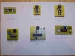
In case anyone is interested, ive made these boards for various picaxe chips so they just plug into breadboard...makes prototyping a bit easier. Download circuit, reverse polarity diode and decoupling cap included on all boards. I still need tomark the supply pins with appropriate coloured paint.
The 5v psu board is still lacking a board mounted switch and the right angle pins for plugging in, but when fitted it will plug into the psu rails on my breadboard.
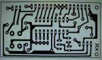
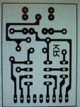
The firmware board is designed to solder to a LCD display in piggy back fashion, incorporating contrast control, reset button and jumpers for the welcome message,baud rate etc. It has a 4 inputs on a latching plug system...+5v, grnd, serial in, lcd backlight control. The backlight can be permanently lit by an on-board jumper if control is not required hence only 3 connections are required. I figured it would be easier to have just 1 board for LCD displays instead of trying to incorporate the firmware chip into various project boards.
The 5v psu board is still lacking a board mounted switch and the right angle pins for plugging in, but when fitted it will plug into the psu rails on my breadboard.
The firmware board is designed to solder to a LCD display in piggy back fashion, incorporating contrast control, reset button and jumpers for the welcome message,baud rate etc. It has a 4 inputs on a latching plug system...+5v, grnd, serial in, lcd backlight control. The backlight can be permanently lit by an on-board jumper if control is not required hence only 3 connections are required. I figured it would be easier to have just 1 board for LCD displays instead of trying to incorporate the firmware chip into various project boards.
Attachments
-
 18.3 KB Views: 428