PICAXE Prog Jack in DIPTRACE

IronJungle

Senior Member
I'm using DIPTRACE (nice package and mega thanks to westaust55 and Myc for the PICAXE focused libraries!).

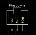
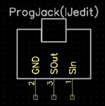
Below is a pic of the programming jack in Myc's library. Assuming the pins are down, there are labeled left to right as:
GND - Ser In - Ser Out

This doesn't make sense to me. It seems like it should be:
GND - Ser Out - Ser In

Am I wrong about this? Is there a way to change the pin labels?

progjack.jpg
 

techElder

Well-known member
Keep in mind that you are building a schematic diagram. You are not creating a physical diagram.

Having said that, this might be a good chance for you to learn how to edit that component. You will also learn how to create your own.
 

IronJungle

Senior Member
Of course, but these libraries are all drawn as physical. For example, the PICAXE ICs etc are all drawn in a labeled pinout fashion. It seems more like an mislabel oversite to me.
 

AllyCat

Senior Member
Hi,

It's probably the symbol for the old "Molex" PICaxe programming header (AXE025) with 3 pins, not the current 3.5mm jack connector.

Cheers, Alan.
 

techElder

Well-known member
I'm still encouraging you to take the time to learn how to do this yourself. You won't be disappointed.
 

MartinM57

Moderator
I've just downloaded Myc's (RIP) library and that schematic symbol has the PCB layout of the normal 3.5mm stereo jack connector.

I also see that the PICAXE chip schematics in his library are "physical" - I have another PICAXE library that has them "logical", which IMHO is preferred as it makes the schematics much clearer, but it's the library writer's choice after all is said and done.
 

westaust55

Moderator
As I recall (not on a PC with DIPTRACE installed at the moment - but at least I have internet on again after a week), mycroft's library has two symbols for the programming socket.

As already suggested, you could just use the component editor part of the DIPTRACE package to edit the pin names to suit your requirements. In this case if you go the next step to generate your own PCB's with DIPTRACE beware the existing pad layouts may also need changing.
 
Top