Light house simulation

69-cat

Member
Hello everyone, Started working with picaxe about 2 months ago mainly for Halloween projects. My wife who loves light houses asked if I could made her one with the simulated beacon using leds. I see some of the PWM circuits but wanted to know how to make it have that simulated "flash" for a short time and ramp back down to "0" and loop.
Dave
 

Rick100

Senior Member
Welcome 69-cat,

I been working on a lighthouse simulator also. Here's a video of my latest version.

http://youtu.be/7lmB5Fk92Qg

It uses an 08M2 and 6 white leds. The leds are wired in opposing pairs. PWM and Charlieplexing are used to ramp down one led while the led next to it is ramping up. I used the DSM to route the PWM to pin C.0 so I could use C.1, C2, and C.4 for Charlieplexing. The leds were from 2 dollar store flashlights. I modified the original flashlight circuit board to use 6 leds instead of the 3. Using PWM looks better than just turning the leds on in sequence although up close it still has a digital look. From a 10 feet away it looks pretty good. Here's the code. It looks long but almost all of it is comments documenting the DSM registers.

Code:
'Simulate rotating beacon like a lighthouse

'switch to select speed on C.3 , enable internal pullup (leg 4)

'pwm from c.2(leg5) routed to C.0(leg 7) with DSM, c.2 is used as normal input and output
'
'
'                                     -anode of led 1 ----
' C.2 (leg 5) to 120 ohm resistor to +                    +- C.0 (leg 7)
'                                     -cathode of led 4 --


'                                     -anode of led 5 ----
' C.1 (leg 6) to 120 ohm resistor to +                    +- C.0 (leg 7)
'                                     -cathode of led 2 --


'                                     -anode of led 3 ----
' C.4 (leg 3) to 120 ohm resistor to +                    +- C.0 (leg 7)
'                                     -cathode of led 6 --


' Physical layout of leds
'
'   1
' 2   6
' 3   5
'   4

' truth table

' H = output High
' L = output Low
' Z = Hi Impedence
'
'      PINS      | led on when PWM
'	C.2  C.1  C.4	1 2 3 4 5 6
'____________________________________
'1	H    L    Z		L H - - - -
'2	Z    L    H		- H L - - -
'3	L    Z    H		- - L H - -
'4	L    H    Z		_ _ _ H L -
'5	Z    H    L		- - - - L H
'6	H    Z    L		L - - - - H


#picaxe 08m2
#no_data

'set up variables

symbol level = w4
symbol lpSpeed =w3


	pullup %00001000	'turn on pullup for C.3

	setfreq m16
	
'the following 4 pokes route the PWM from c.2 to c.0 and allow c.2 to be used as normal input/output
'the pwmout and pwmduty commands still need to address c.2

	pokeSfr $FC, %11000001 ; SFR $39C MDCON (mixer turned on and output of mixer on MDOUT , leg 7 enabled)
	'MDCON: MODULATION CONTROL REGISTER
	'bit 7 MDEN: Modulator Module Enable bit
	'	1 = Modulator module is enabled and mixing input signals
	'	0 = Modulator module is disabled and has no output
	'bit 6 MDOE: Modulator Module Pin Output Enable bit
	'	1 = Modulator pin output enabled
	'	0 = Modulator pin output disabled
	'bit 5 MDSLR: MDOUT Pin Slew Rate Limiting bit
	'	1 = MDOUT pin slew rate limiting enabled
	'	0 = MDOUT pin slew rate limiting disabled
	'bit 4 MDOPOL: Modulator Output Polarity Select bit
	'	1 = Modulator output signal is inverted
	'	0 = Modulator output signal is not inverted
	'bit 3 MDOUT: Modulator Output bit
	'	Displays the current output value of the Modulator module.(1)
	'bit 2-1 Unimplemented: Read as ‘0’
	'bit 0 MDBIT: Allows software to manually set modulation source input to module(1)
	'	1 = Modulator uses High Carrier source
	'	0 = Modulator uses Low Carrier source
	
	pokeSfr $FD, %00000000 ; SFR $39D MDSRC
	' modulator source is MDBIT , software control
	'MDSRC: MODULATION SOURCE CONTROL REGISTER
	'bit 7 MDMSODIS: Modulation Source Output Disable bit
	'	1 = Output signal driving the peripheral output pin (selected by MDMS<3:0>) is disabled
	'	0 = Output signal driving the peripheral output pin (selected by MDMS<3:0>) is enabled
	'bit 6-4 Unimplemented: Read as ‘0’
	'bit 3-0 MDMS<3:0> Modulation Source Selection bits
	'	1111 = Reserved. No channel connected.
	'	1110 = Reserved. No channel connected.
	'	1101 = Reserved. No channel connected.
	'	1100 = Reserved. No channel connected.
	'	1011 = Reserved. No channel connected.
	'	1010 = EUSART TX output.
	'	1001 = Reserved. No channel connected.
	'	1000 = MSSP1 SDO output
	'	0111 = Reserved. No channel connected.
	'	0110 = Comparator 1 output
	'	0101 = Reserved. No channel connected.
	'	0100 = Reserved. No channel connected.
	'	0011 = Reserved. No channel connected.
	'	0010 = CCP1 output (PWM Output mode only)
	'	0001 = MDMIN port pin
	'	0000 = MDBIT bit of MDCON register is modulation source
	
	pokeSfr $FE, %00000000 ; SFR $39E MDCARL
	'when the modulating signal is low the output on MDOUT will be 0
	'MDCARL: MODULATION LOW CARRIER CONTROL REGISTER
	'bit 7 MDCLODIS: Modulator Low Carrier Output Disable bit
	'	1 = Output signal driving the peripheral output pin (selected by MDCL<3:0> of the MDCARL register)
	'	is disabled
	'	0 = Output signal driving the peripheral output pin (selected by MDCL<3:0> of the MDCARL register)
	'	is enabled
	'bit 6 MDCLPOL: Modulator Low Carrier Polarity Select bit
	'	1 = Selected low carrier signal is inverted
	'	0 = Selected low carrier signal is not inverted
	'bit 5 MDCLSYNC: Modulator Low Carrier Synchronization Enable bit
	'	1 = Modulator waits for a falling edge on the low time carrier signal before allowing a switch to the high
	'	time carrier
	'	0 = Modulator Output is not synchronized to the low time carrier signal(1)
	'bit 4 Unimplemented: Read as ‘0’
	'bit 3-0 MDCL<3:0> Modulator Data High Carrier Selection bits (1)
	'	1111 = Reserved. No channel connected.
	'
	'	0101 = Reserved. No channel connected.
	'	0100 = CCP1 output (PWM Output mode only)
	'	0011 = Reference Clock module signal
	'	0010 = Reserved. No channel connected.
	'	0001 = MDCIN1 port pin
	'	0000 = VSS
	
	pokeSfr $FF, %10000100 ; SFR $39F MDCARH
	'when the modulating signal is high the output on MDOUT will be the CCP1 (pwm)
	'the pwm signal will not drive the output pin (leg 5) so we can use it as an adc (hopefully)
	'MDCARH: MODULATION HIGH CARRIER CONTROL REGISTER
	'bit 7 MDCHODIS: Modulator High Carrier Output Disable bit
	'	1 = Output signal driving the peripheral output pin (selected by MDCH<3:0>) is disabled
	'	0 = Output signal driving the peripheral output pin (selected by MDCH<3:0>) is enabled
	'bit 6 MDCHPOL: Modulator High Carrier Polarity Select bit
	'	1 = Selected high carrier signal is inverted
	'	0 = Selected high carrier signal is not inverted
	'bit 5 MDCHSYNC: Modulator High Carrier Synchronization Enable bit
	'	1 = Modulator waits for a falling edge on the high time carrier signal before allowing a switch to the
	'	low time carrier
	'	0 = Modulator Output is not synchronized to the high time carrier signal(1)
	'bit 4 Unimplemented: Read as ‘0’
	'bit 3-0 MDCH<3:0> Modulator Data High Carrier Selection bits (1)
	'	1111 = Reserved. No channel connected.
	'
	'	0101 = Reserved. No channel connected.
	'	0100 = CCP1 output (PWM Output mode only)
	'	0011 = Reference Clock module signal (CLKR)
	'	0010 = MDCIN2 port pin
	'	0001 = MDCIN1 port pin
	'	0000 = VSS

	'=============================================

	pwmout pwmdiv16, c.2, 249, 0	'1000 Hz @ 16MHz clock / 0 - 100% = 0 - 1000 pwmduty counts
	dirsC = %00111

top:

	if pinC.3 = 0 then	'select slow or fast speed
		lpSpeed = 10
	else
		 lpSpeed = 150
	endif

'step 1 pin setup
	outpinsC = %00100
	dirsC = %00111

	gosub rampUp

'step 2 pin setup
	dirsC = %00011		'make the pin were about to change HI-Z first or we'll se it flash
	outpinsC = %10000
	dirsC = %10011
	
	gosub rampDown

'step 3 pin setup
	outpinsC = %10000
	dirsC = %10101
	
	gosub rampUp

'step 4 pin setup
	dirsC = %00101		'make the pin were about to change HI-Z first or we'll se it flash
	outpinsC = %00010
	dirsC = %00111
	
	gosub rampDown

'step 5 pin setup
	outpinsC = %00010
	dirsC = %10011
	
	gosub rampUp

'step 6 pin setup
	dirsC = %10001		'make the pin were about to change HI-Z first or we'll se it flash
	outpinsC = %00100
	dirsC = %10101
	
	gosub rampDown
	
	goto top

rampUp:
	for level = 0 to 1000 step 20
		pwmduty c.2,level ; set pwm duty (actually shows up on c.0)
		pause lpSpeed
	next level
	return	'rampUp

rampDown:
	for level = 1000 to 0 step - 20
		pwmduty c.2,level ; set pwm duty (actually shows up on c.0)
		pause lpSpeed
	next level
	return	'rampDown
lighthouse.png

Good luck,
Rick
 
Last edited:

techElder

Well-known member
I started out thinking, one day a long time ago, that I needed a light for every so many degrees. Then I got to staring at a video of a lighthouse on a clear night. Eureka! From anywhere you stand it looks the same.

So, I used ONE light and a multi-slope ramp. From any direction it has that lighthouse "flash." It does help some to find a "lens" that has some facets on it. Makes it look a little better.

Mine was built with a 120 VAC bulb. I modified a common lamp dimmer to accept my ramp generated from a DAC. There isn't any reason you can't do the same with a PICAXE, PWM and LEDs.
 

69-cat

Member
Thank you.... I now have 2 options for larger and smaller light houses. She has a smaller light house that the single LED would be great in. All I have to do is drill all of the way to the top outour coming through the side:rolleyes:
Dave
 

raits999

Member
Years ago in school i made lighthouse using 555 timer and 4017 logic that drives 20 leds.
LIghthouse.jpg
If you add caps to the outputs you can have nice trail.
 

FunFlyer

New Member
Very interesting little setup! looks great. I built it using 20mA LEDs. But using the pins of the 08M2 directly doesn´t give much current to work with. In a "normal" setup one could just a MOSFET to boost the output power. I don´t think this would work in this case, since the pins are used as tristate. Any suggestions on how to solve this?
 

AllyCat

Senior Member
Hi,
Very interesting little setup! looks great. ..... But using the pins of the 08M2 directly doesn´t give much current to work with. ....
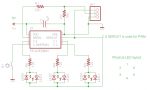
Presumably you're referring specifically to Rick100's design in post #3? Those POKESFR's are quite "advanced" programming and might not be trivial to convert to even another PICaxe*. That also makes it quite difficult to predict how the design might best be adapted for a brighter output, so I'd start with KISS (Keep It SimpleS). The 120 ohm resistors can probably be (safely) reduced, because the LEDs are bridged between a HIGH and a LOW PIC(axe) output pin, the current will be limited by the Pull-Up FET (which is always "weaker" than the Pull-Down). With a supply rail of 4.5 volts or less the resistor can probably be removed entirely (short-circuited), but for a higher voltage it might be wise to try a few resistor values to achieve the maximum 25 mA rated output pin current. If that's still not bright enough then maybe look for some more efficient white LEDs. ;)

Indeed, it's not easy to add external FETs to emulate a Tri-state output, but it might be possible if suitable (complementary) FETs can be found (or selected) with an actual gate-source cut-off voltage of just greater than half the supply rail (e.g. 3 volts Vgs). However bipolar transistors do have a more predictable On/Off base-emitter voltage threshold around 500 mV, so it might be practical to add a voltage divider resistor network (approximately 4R / R) to each base (NPN and PNP), but it's unlikely to be very efficient, with several mA flowing in each divider even when the driven transistor is Off.

* Personally, I'm not convinced that the remapping of the PWM via the DSM to C.0 is essential, because at the PIC hardware level the drivers to Legs 7 and 5 (PICaxe C.0 and C.2) are basically identical and the PICaxe OS might not seriously undermine this, particularly if writing to the ports directly via SFR commands. Although "officially" C.0 is defined as "Output Only", in practice it can be Tri-Stated at least via the READ
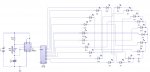
DAC command. Also, IMHO the LEDs are not strictly being driven as a Chalieplex, which could drive 12 LEDs from 4 output pins (even with brightness control, at least via software/multiplexing). However, alternate LEDs must be wired Anode/Cathode to the "PWM" Output so that one increases in brightness whilst the adjacent LED reduces. Incidentally, since the aim is to produce a "rotating" result, I can't decide if the effect might be any better if the PWM sequence was sinusoidal (which could be easily implemented via a lookup table) rather than a simple Ramp Up/Dowm. It might depend on the particular LEDs' Beam-Width/Pattern?

Cheers, Alan.
 

hippy

Technical Support
Staff member
Personally, I'm not convinced that the remapping of the PWM via the DSM to C.0 is essential
Possibly and it may just have been the easy option; allow what is 'output only' to be used as a PWM output leaving the other I/O pins to be easily tri-stated as needed.

While it may be possible to tri-state C.0 I can't say I have tried that and there may be hidden gotchas with doing that while re-routing PWM to C.0 has been proven to work. But, if it does work, one could alternatively do it that way.
 
Top