Help:parallel in to serial out shift register

hisem

New Member
Hi, I hope this is the correct place to post this question. I am hoping someone can help me. I need someone to explain (in simple terms), how to set up a parallel in to serial out shift register to an 08M/18X, and how the 08M/18X should be coded to read all the inputs. I would like 16 inputs initially, but would like to expand as needed.

Here is my idea:
08M/18X only sits and waits for a request as interrupt on serial bus from other picaxe chip. when receives request for info, 08M/18X checks state of all inputs, deciphers info, sends back info to other picaxe on serial bus. It's essentially a self diagnostic system. 1 picaxe waits for other to request state of this or that system, when received request, it checks and tells the other picaxe what is what, then continues to wait for next request. So far I have 12 high/low points to check, but will have more. speed is of no real issue either.(it can take as long as it takes)

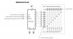
Also if anyone could provide a basic schematic as to the hookup of the shift register to the picaxe that would be great:)

I know of 2 chips that can do this, 4014 and 74HC165. which one I should use I don't know, but I understand that there isn't much difference.I may be wrong.

Any and all help much appreciated.
Thanks
 

westaust55

Moderator
parallel in to serial out shift register

Welcome to the PICAXE forum.


Both chips you mention can do the same task however they are not pin for pin compatible nor a drop in replacement for each other. Suspect that the 74HC165 has seen more discussion.use her in the past.

You can use the 74HC165 shift register to obtain and input 8 bits of data. You could also cascade these and each added 74HC165 will enable you to enter a further 8 bits of data.

Have a look at the attached diagram


Have a look at the program code examples for SHIFTIN capabilities in PIACXE Manual 2 bottom of page 189 onwards.

Good so far and the program code is relatively easy, but (there is always a catch :rolleyes: ) there is no way that the 74HC165 can provide a signal to the PICAXE to indicate when there is data to be loaded.


An alternative:

You could consider the MCP23017 i2c IO expander chip. This can handle 16 signals with a single chip.
This will work with the PICAXE 18X which has inbuilt i2c comms :) but not the 08M :( (and by the time you created i2c code in an 08M there would be virtually no space left to do anything else).

The MCP23017 has the ability to interrupt the PICAXE chip when any of the inputs has changed state.


Before folks here can help you much further you need to decide if/why you do need an interrup to have the PICAXE load in the data/signals
and whether the MCP23017 might be a better option in conjunction with the 18X.

You can also do a search of this forum for 74HC165 and MCP23017 and will find quite a few threads with reference to these chips.
 

Attachments

Last edited:

hisem

New Member
Hi westaust55, thank you fot your reply :)
Let me clairify what is going on and what i'm trying to do.

The 08M is connected to multipile other pixaxe chips along a serial comunications bus on pin 4. it waits for another picaxe chip to to pull pin 4 low indicating there is an incomming message. When the interrupt occurs, the serin command is fired. The message itself is 3 bytes: the number of the chip the message is for, followed by two bytes that make up a word variable indicating the message. In this case "Check state of all pins and report state back" 08M then and only then checks the state of the input pins from the 74HC165(s), reports that state back up the bus to another picaxe chip, resets the interupt on pin 4, and sits and waits for another request from an other picaxe chip to do it again. While it is waiting the state of the pins connected to the 74HC165 (s) can change as much as they want. I will only need to know the state at the moment of request from a separarte picaxe chip requesting the 08M to look and see.

Your diagram seems quite straight forward and I have read the pages you sugested in manual 2, but I am confused about pin 1 on the diagram(picaxe output to latch data). Do I need to connect this to the 08M in my aplication? what is this for? Do I not just need the clock and data out from the 74HC165? and if so what do I do with pin 1, leave it floating or tie it high/low?

As far as the programming goes i'm unsure, would it look something like this:

symbol sclk = 5 ‘ clock (output pin)
symbol serdata = input6 ‘ data (input pin for shiftin)
symbol counter = b7 ‘ variable used during loop
symbol mask = w4 ‘ bit masking variable
symbol var_in = w5 ‘ data variable used durig shiftin
symbol bits = 12 ‘ number of bits
symbol MSBvalue = 2048 ‘ MSBvalue

shiftin_LSB_Pre:
let var_in = 0
for counter = 1 to 12
var_in = var_in / 2
if serdata = 0 then skipLSBPre
var_in = var_in + MSBValue
skipLSBPre: pulsout sclk,1
next counter
return

Once again, Thank so much for all your help :)
 

westaust55

Moderator
Okay understand where the interrupt comes into play now.

The 74HC165 will tentatively do what you want.

The latch pin/signal is required with the 74HC165, as the parallel input data is only accepted into the shift register when the voltage level on that pin (latch/load) drops form a high state to a low state. It cannot permanently be held high or low.

The reason for this latching/loading of the data is to accept data at a specific point in time and clock this out. Without a latch/load function, the input data could be dynamically changing as you try to shift the data into the PICAXE leading to erroneous data. Would also be a problem even if not dynamically changing as when you shifted the data along, another input would overwrite the data form a lower bit as it shifted through the shift register.
 
Top