Hi,
Hopefully one day i might actually be able to help people and answer questions rather than always asking them and taking up your time
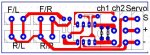
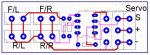
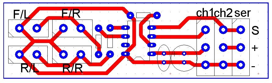
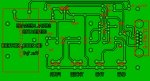
I built a indicator circuit for one of my model trucks. I have it working on strip board, and now i want to attempt getting it onto pcb.
I have designed the pcb layout, and just wondered if one of you would mind checking it for me, and seeing if it looks ok....more component placement and routing.....
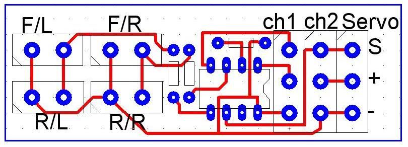
ch1 - RC reciever channel 1 - one push up makes all 4 leds flash (hazard lights)
ch2 - RC reciever channel 2 - steer left/left leds - steer right/right leds
Servo - To the steering servo...
resistor near picaxe is a 10K serial one (i remembered )
other 2 are for the leds and are 56k
I decided to connect off the board as i have a load of extension cables i can cut in half rather than use Y cables.
hope this makes sense... and i really appreciate any comments good or bad
thanks
Hopefully one day i might actually be able to help people and answer questions rather than always asking them and taking up your time
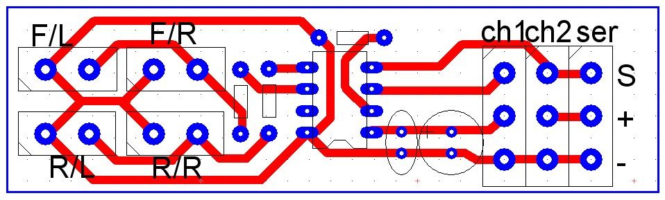
I built a indicator circuit for one of my model trucks. I have it working on strip board, and now i want to attempt getting it onto pcb.
I have designed the pcb layout, and just wondered if one of you would mind checking it for me, and seeing if it looks ok....more component placement and routing.....
ch1 - RC reciever channel 1 - one push up makes all 4 leds flash (hazard lights)
ch2 - RC reciever channel 2 - steer left/left leds - steer right/right leds
Servo - To the steering servo...
resistor near picaxe is a 10K serial one (i remembered
)other 2 are for the leds and are 56k
I decided to connect off the board as i have a load of extension cables i can cut in half rather than use Y cables.
hope this makes sense... and i really appreciate any comments good or bad
thanks
Last edited: