Did I damage My pic?? (2x)

Lt2mc

Member
Hey all,
I am back on my LED test project, after an 18 month TBI induce hiatus, enough said, I am now trying to get back up to speed, with more help from you all.

for some back ground,
This is the same project i was working on back in 2019, and everyone helped me get the Hi2c DAC working. I have now had a chance to run full scale testing in my machine, and discovered the LED wont shut off with a Hi output from Pin B.6.
My program appears to be working (on the simulator). however after extensive diagnostics with the pic on my PCB, I found I cannot get two of my outputs to trigger hi (pin B.5, and B.6) at least when I measure for 5v on the cable leading to the transistors i am trying to trigger. So far i have tried two different 28x2 pics, and i find it hard to believe both chips have been damaged in the same way, so far the rest of program works as expected on the board, using both chips.
Any thoughts?

I will be presumptuous and post the Code I have so far, ragged as it is;
 

Attachments

J G

Active member
Hello,
To test, can you put the picaxe chips in a separate breadboard and power supply and flash a simple program with the sole purpose of testing the pins to doubly make sure it isn't a logic issue in your more complex program or a short somewhere on the pcb stopping the pins from going high?
i.e.

Code:
main:
    sertxd("Setting pins HIGH", cr, lf)
    high B.5
    high B.6
    pause 10000
    sertxd("Setting pins LOW", cr, lf)
    low B.5
    low B.6
    pause 10000
    goto main
Hope this helps.
 

AllyCat

Senior Member
Hi,

To answer the title ....... Probably not.
... I cannot get two of my outputs to trigger hi (pin B.5, and B.6) at least when I measure for 5v on the cable leading to the transistors i am trying to trigger.
A schematic might be helpful, but the first obvious question is "Have you remembered to put resistors in series with the transistor Base inputs?". Unlike a FET, the input base-emitter junction appears as a forward biassed diode so cannot rise above about 600 mV.

I must admit that I haven't bothered to download and examine your program in detail; it would be much easier if posted between [code ] [/code] tags.

Cheers, Alan.
 

Lt2mc

Member
Thanks everyone for the inputs, (pun Intended). To clarify when I am testing for my outputs , I have isolated the IC from that specific leg of the circuit, and am checking for voltage at the ic leg directly. Should I test the leg using a 1k load on my meter lead?

Here is the pcb diagram describing what my intent is with the output B.6.
As a circuit sanity check i did apply 5v directly to pin 2 of DAC in (Pin B.6 disconected), and the circuit functioned as expected, albeit in the reverse of what I thought, i.e a high at Q1 turned off the LED driver via Q2
I will definetly get back to the basics, and bread board this circuit in the morning.
BTW, sorry about not doing the Code to code post, the intial posting didn't like it since it was > 10k characters. The prog is fairly short, I just like to comment my code in detail. ;)
24435 circuit
 

premelec

Senior Member
Not sure what you are getting a DAC signal from... if from PCAXE I don't see any dacsetup in code and also note that the signal from PICAXE is soft [high impedance] - specifically to be used with amplification...
 

AllyCat

Senior Member
Hi,
...... Code to code post, the initial posting didn't like it since it was > 10k characters. The prog is fairly short, I just like to comment my code in detail. ;)
You might need to avoid the "Copy for Forum" option in the PE because I believe it adds an enormous number of [COLOR= ] instructions. Certainly I am also renowned for exceeding the 10k character limit in my "finished" program listings, but it should be possible to "strip down" a program to demonstrate a specific problem or bug.

Your use of the term "DAC input" may be causing (us) confusion. The PICaxe has both a DAC (output) and multiple ADC inputs. Do you mean the signal is an input from another (external) DAC, or an ADC input , or something else? Actually, the PICaxe DAC has a very high output impedance, so it can be used as an input (under very special conditions), but this is rarely done because in most M2s it is shared with the Serial/Programming Output pin.

No, you shouldn't need to use a (1k) "load" resistor for testing any normal PICaxe output pin. But sometimes, a resistor in series with a probe can be wise if using a multimeter that can be easily switched between Voltage and Current ranges. ;)

Cheers, Alan.
 

Goeytex

Senior Member
If I assume that Q1 is an NPN transistor and that Q2 is an N-Channel Mosfet then it appears that
The MOSFET Gate is being Pulled up to 24V via R2 (Value unknown). So ...when PICAXE B.6 goes High
Q1 turns on taking the gate to Ground turning off the Q2 FET.

Many(most?) FETS cannot take 24V on the Gate. Is Q2 Rated at > 24V Gate to Source Voltage?
Is Q2 Possibly "Blown" .


If Q2 is indeed an N-Channel MOSFET, then a better approach might be to use a Mosfet Driver.
At the very least the voltage to the base of the FET should be reduced to about 12V (Depending upon the FET). This
could be done with a voltage divider instead of a single pull up resistor.

Of course my wild speculations could be totally wrong. But we have no schematic diagram or component descriptions.
A schematic would be much more useful than a board layout for diagnosing issues like this. That way
folks don't have to make crazy assumptions and wild guesses.
 

Lt2mc

Member
thanks for all the inputs. If I showed you my schematics/cave drawings their would definitely be more confusion, since napkins and crayons dont scan so well. So far the assumptions are accurate, Q1 is a NPN (3904), and Q2 is a N-channel Mosfet (Fqp30N06). The idea of a voltage divider sounds interesting, I will have to add that to my revision list.

As for the DAC signals, I originally tried using the pic's on board stuff, but in turn decided I needed better resolution, so I went with a Gravitech i2c DAC Daughter board, which gave me an almost 2x increase in resolution. Thanks Hippy and others for helping with that part of the project.

Premelec, I am a little concerned about your statement regarding possible High impedance, I have been a low voltage DC controls type guy my whole career, and every time some one says High impedance, I think it is a fancy way of saying high resistance. What exactly do you mean?, or can you point me to resource that will explain it in relation to this type of circuit? That is what is so fun about this stuff, learning new things with every project.
 

premelec

Senior Member
Impedance pretty much just recognizes that capacitance and inductance may be involved as well as resistance. In your case likely not of much consequence... what you want is source resistance from the DAC output... the datasheet says there is a buffer amp but I didn't see any spec on what the drive current etc is available. AND we still don't have your specific circuitry that you are trying to drive from the DAC board. I guess since you have tested that your circuit works with voltages inputted you can play empiricist and add series resistance to your test and see if it still drives ok. And test if proper DAC signals are coming from the DAC board... I built some 8 channel LED drivers using a TI 8 channel DAC - [about a decade ago] worked fine [still does - I bit banged Data and Clock w/08M2]. If you are just trying to vary current in LED slowly you might consider simply using a MOSFET with a small resistor from source to V- which will give you current information and drive the gate through RC filter with PWMOUT noting the current with READADC pin on the MOSFET source to V- . The MOSFET will take full voltage and current [need heat sink? don't know the currents you are using]. If you still have trouble let us know...

Pay attention to what Goeytex said - if your DAC goes directly to a BJT base that has emitter to V- that won't work out well... Please do post a circuit - picture of it chalked on a sidewalk if you wish - I' not picky... ;-0
 
Last edited:

tmfkam

Senior Member
As it looks, when the input from the DAC is above 0.7V, Q1 will turn on and Q2 will turn off (or on). When the input from the DAC is below 0.7V the opposite will occur. Q1 and Q2 seem to be configured as switches.

If your intention is to have Q2 turn on in proportion to the level of voltage applied to DAC in, you are going to need a linear output stage. Something entirely different.
 

AllyCat

Senior Member
Hi,
As for the DAC signals, I originally tried using the pic's on board stuff, but in turn decided I needed better resolution, so I went with a Gravitech i2c DAC Daughter board, which gave me an almost 2x increase in resolution.
As others, I'm "confused" with what you're trying to achieve with the "DAC". The circuit (Q1 + Q2) that you show is a digital amplifier and certainly won't accurately amplify an Analogue signal.

The PIC(axe) "DAC" is rather a misleading name, it's basically just a low resolution "bias" (resistive divider or potentiometer) network, particularly useful for the on-chip comparator(s). It has only 32 output levels (5 bits) so your "almost 2x increase in resolution" (to 64 levels) still seems very poor. Even doubling the number of bits (i.e. to 10 bits) would give only 1024 levels, which is not difficult achieve even with the most basic modern PICaxe:

The PICaxe PWM output(s) have 10-bit resolution and often can be used as a "DAC", for example to dim one or more LEDs, either directly or via a (digital) driver/amplifier. In this case the LED(s) are rapidly switched on and off and the (human) eye "integrates" (or filters) the brightness; but the output resistance (or impedance) can be very low. For other applications where a "genuine" analogue level is required, then the PWM can be Low-Pass filtered to give as smooth a voltage level as desired. A simple Resistor-Capacitor filter will have a higher output resistance (that can be improved in many ways if necessary) and a "slower" response. But the update rate via an I2C bus from a PICaxe is not going to be "fast".

One potential limitation of a basic "PWM DAC" is that the output voltage is "ratiometric" (i.e. varies) with the supply voltage, whilst a "normal DAC" may include a (Fixed) Voltage Regulator. However, there are various ways to work around this issue and some years ago I posted a "Finished Project" which could give an 8-bit regulated (compensated) DAC output voltage from almost any PICaxe, using (only) the internal PWM and FVR.

Cheers, Alan.
 

Lt2mc

Member
Ok back to another weekend of bit bashing, today's efforts found 3 bad/damaged/burned up 28x2s. So Long post short I did damage my PICs. Thanks to JG's suggestion, I broke out the bread board and rigged up an led output test for my suspected bad PICs, verified with some known good 28x2s. Long story short I loaded the original prog onto a new PIC (also tested on the bread board), and every thing works like it should. :)
for those interested in the bigger picture, here is the best I can do, explaining how every thing works, yes another PCB lay diagram. Q1 and Q2 are essentially power switches for the 24vdc LED driver power ( I call them shutters in the program so others in my group can visualize the shutters that currently block the mercury lamps i hope to eventfully replace. The DAC in signal (pin#3) is a 0-10v Alog signal generated by a gravitech Hi2c DAC module located off board from this diagram. It's purpose is to brighten or dim the 265nm LEDs i am testing. I hope this helps.
BTW Does anyone have a suggestion for a low cost easy to learn schematic drawing app?
24454

:)Again, Thanks for the idea of a voltage dividers. I found several places I can incorporate one, not only on this pcb, but else where in my design.
 

J G

Active member
So Long post short I did damage my PICs
If you don't need to use all the pins, can you move the pins required off to another port or use them in another project (make sure to mark which pins are dud) seeing as the processor itself still seems ok.

BTW Does anyone have a suggestion for a low cost easy to learn schematic drawing app?
I have been having a go with KiCAD recently, which is open source. It seems quite nice to use. I like the separation of footprint from schematic symbols as then I only have to worry about PCB stuff later on. I have also used Eagle in the past. Not sure if it still exists, but there was / is a free version for hobbyists with a limited number of layers and board size. For both of these, there are a lot of tutorials online.

Otherwise, you could use something like LucidChart, slideshow software or Inkscape to manually draw things out, but that might drive you mad doing so :).
 

Goeytex

Senior Member
@Lt2mc

Originally you inidicated that the FET was FQP30N06. Now we see that it is a FQP30N06L. The L version is a logic Level FET with a max Gate to Source voltage of 16V. You are applying 24V with this circuit, most likely damaging the FET.

We cannot see how the Picaxe is connected to the rest of the circuit based upon what you have provided. So there is not much anyone can do to help you solve your problems give the lack of relevant information.

There are many qualified and experienced people here that are willing to help you solve your issues. However you need to be willing to do your part to provide accurate and relevant information.

Please provide a complete schematic, even if you have to draw it by hand.
 

tmfkam

Senior Member
I see. The "DAC" signal seems to be fed to the LED driver module, and a secondary signal is connected to the transistor pair. That may have more chance of working (assuming the 24V issue Goeytex mentions is adjusted). Most LED drivers I've seen can be dimmed using PWM though, which might be easier?
 

Goeytex

Senior Member
I drew up a diagram that represents the circuit as Lt2mc has described it. I added decoupling capacitors and Pullups for the I2c lines. As drawn, the 24v applied to the FET Gate will most likely blow the FET. I also added a 1000uf bulk capacitor near the LDD-1500. This may or may not be needed, but I would probably use it.

The Gravitech I2C DAC is 8 bit so I am guessing that with a 0-255 value input there should be a 0 - 5V output. However, the LDD-1500 specifies .5V to 2.5V (Full Range) . This will need to scaled to operate correctly. Consider a voltage divider.

IT may be important to note that the LDD-1500 input will also accept a PWM input for dimming. The PWM input to LDD-1500 (Pin 21) is specified to be between 100 and 500 Hz.

When the LDD-1500 input is below .5V the output will shut off. So I am confused about the need for the MOSFET. With nothing connected to LDD-1500 the output will be full on.

Unless I am misreading the datasheets or misunderstanding what the circuit is supposed to to, it seems to me that the NPN Transistor, Mosfet and DAC can all be eliminated and the LDD-1500 can be controlled with a Picaxe PWM Output directly applied to LDD-1500 (Pin21). 100 Percent Duty will be full on. 0% Duty will be full off, or you could just turn the PWM OFF ( assuming the PWM pin will be low). See the LDD-1500 Datasheet

The PWM range will depend upon the current capability of the 265nm UVC-LED. Full on will be ~1.5 amps. 50% duty will be ~750 ma.

A diagram is attached for markup and correction. Just open it in MSPAINT and have at it.

Goeytex
 

Attachments

Lt2mc

Member
Dang Guys, It looks like I am working with the big kids now, and it is humbling. This has always been a kind of rouge project at my day job, so it is very enlightening to finally get some solid critical feed back.

As for the simpler PWM control. I had to rule out PWM control early on in the project, since the sensorisation I am forced to use, will not accurately report a light source's power output being controlled by the on/off oscillations of a PWM signal. This project is ultimately intended to replace the mercury lamps used in a photo-lithography tool, whose power is controlled by various mechanical shutters and apertures. So I am constrained by the control loop currently in place, which early experiments showed would oscillate wildly using a PWM LED control.

Thanks Goeytex for all the information, and diagram, it is like getting my homework back, with no grade, and a "Finish corrections, resubmit" ;)
Which is not a bad thing, it just means I need to sit down and do some serious review.

Btw I will also have to review my notes and see how that FQP30N06L-ND made it into the mix.
Final note, I down loaded KiCad, and will give it a try, as part of my review process.
 

premelec

Senior Member
It is not clear to me that the current output to the LED will show the PWM current module control input... more likely some ripple from the current regulator module internals; in any case that could be filtered at the output depending on how fast you need to change currents. If you want clean DC current that can be done with a linear amplifier and DAC with some loss of power efficiency.
 

tmfkam

Senior Member
... in any case that could be filtered at the output depending on how fast you need to change currents.
Or the sensors could be filtered? Either with some capacitance added to the sensor inputs or by averaging a few readings.
 

Goeytex

Senior Member
As I read the LDD-1500 Datasheet with an analog input on Pin 21 the output is constant current by way of DC Step Down Converter. The ripple is specified at Max 1.5V. However a note on Page 5 States:

◎ During PWM dimming operation, the output current will change to PWM style.

So non-PWM with analog dimming and PWM with PWM Dimming. That is how I read it.

What I do not understand is the need for Q1 and Q2 to enable or disable the LD-1500 by switching the Ground on or off. And why the MOSFET gate is pulled up (ON) by default. The LDD-1500 can be turned off by sending a value of 0 to to the DAC and can be turned on full by sending a value > 128 to the DAC. In the OFF state the the quiescent Current is is only about 4 ma.

So maybe Lt2mc can explain this.

Further, I see nothing in the circuit I posted that would cause the PIC to blow. The FET, yes. But the circuit diagram is incomplete and Lt2mc does not seem too keen on supplying a complete and accurate circuit for proper analysis.
 
Last edited:

AllyCat

Senior Member
Hi,
So non-PWM with analog dimming and PWM with PWM Dimming. That is how I read it.
Not quite, IMHO. "Analogue Dimming" would involve a large power dissipation in the LDD-1500, which I don't believe such a small device could tolerate. At the extreme, the specification mentions a maximum input voltage of 36v and an output of 1 Amp into a 2 volt diode. That implies an "analogue" dissipation of 34 watts in the LDD-1500! :eek:

My reading of the data sheet is that the device has four "modes": OFF , ON , internal PWM (analogue dimming) and "brute force" (ON/OFF) dimming (but still using internal PWM to reduce the power dissipation). So, as Goeytex says, the transistors Q1 and Q2 (and the use of a DAC-derived analogue input) seems completely unnecessary.

This isn't the place for a complete "tutorial" on PWM, but IMHO this thread contains (at least) three fundamental misunderstandings: Firstly, even a humble PICaxe can generate PWM frequencies between less than 100 Hz to over 1 MHz, that's a ratio of over 10,000 : 1 and most electronics components will behave very differently over that range (compare with what you might be able to do in one second against 3 hours!). Secondly, there is the difference between the "Interface" specification and the "Output" Operation/Mode: For example, a modeller's "Servo" which uses a Width-Modulated Pulse Interface, but has an Analogue (position) Output. Finally, there is the absolutely fundamental difference of whether the (PWM) Output Load is Resistive or Inductive; But note that there may be (Inductive or Resistive) Low-Pass filters "hidden" in modules such as the LDD-1500.

Firstly, consider simple LED dimming with a resistive load; for example two 3 volt LEDs in series with a 60 ohm resistor across 12 volts: A current of 100 mA will flow, giving a power of 600 mW in the diodes (together) and another 600 mW dissipation in the resistor, an "efficiency" of 50%. Switch that on and off rapidly with a 50% duty cycle "PWM" (at almost any frequency) and the average current will fall to 50mA, with halved (average) dissipation in the LEDs and Resistor. The peak current is still 100 mA but the (human) eye will see a lower brightness because it averages the brightness (i.e. it is a low-pass filter).

However an inductive load is completely different: The PWM frequency becomes very important; at 100 Hz most (small) inductors will just behave like a resistor (since they are wound with resistive copper wire), whilst at 1 MHz they may virtually "look" like an open circuit. But at the "design" frequency, when the (PWM) Output Voltage is "High", the current gradually increases in the circuit; there must still be 6 volts across the LEDs, so also 6 volts across the inductor, but it doesn't "dissipate" (much) power; instead it stores the energy in its magnetic field. Then during the PWM OFF period, the current continues to flow (via the essential "flywheel" diode), gradually reducing. Nearly all the energy is recovered from the inductor and applied to the LEDs (since the voltage across the inductor is now reversed). There can still be an average 50 mA flowing in the LEDs, but only 25 mA average (50mA for half of the time) from the supply, thus almost 100% efficiency.

But the user doesn't need to "know" about all of this (which is the basic principle of any PWM power supply), because the inductor is hidden in the module: with correctly chosen components the output can just "look" like a constant voltage and current (which effectively it is). The same can apply to the "Analogue" input, a simple Low-Pass filter can be inserted to convert (i.e. average) the PICaxe's PWM signal to create an analogue input. Then the (essential) PWM Modulator inside the LDD-1500 generates its own "internal" PWM signal at a very high frequency (the data sheet says 1 MHz) to permit it to use small inductance and capacitance values.

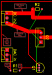
Finally, an observation on the "DAC" input to the PCB: It appears to have an Analogue signal input (although it's driving a digital amplifier !) and an "Enable" input, but NO Earth ! An analogue input should always have a partner Earth (even if it may be later decided that it's necessary to break an "Earth Loop" for good "audio" quality ;) ).

Cheers, Alan.
 

premelec

Senior Member
Not sure where the LDD-1500 module was called out by OP but if in use according to data sheet ref by Tex looks like 1 MHz internal switch rate.... what is not clear in this interesting project is what precision is needed and how fast the output to the LEDs needs to change and stabilize... perhaps OP can clarify requirements...
 

Goeytex

Senior Member
I think that it is incorrect to assume that the output of the LDD-1500L is strictly a PWM. It seems rather clear to me that with an analog control voltage on the input pin that the output is constant current relative to the input control voltage.

This is the way other similar drivers operate eg. The LuxDrive 3021 BuckPuck. I might be wrong, but I imagine this is why the OP selected this particular driver.

Being a DC to DC converter with an efficiency of up to 95%, the heat dissipation requirement of the controller will be minimal. "Analog dimming" in this case simply means than an analog input (control voltage) is used to set the current limit of the DC to DC converter.
 
Top