Circuit works fine with 18M2, but not with an 08M2?

GenericEvilGenius

New Member
So I have a test circuit that consists of 16 LEDs, driven by a pair of 74hc595N shift registers, and controlled by an 18M2. It works perfectly, but when I try changing the 18M2 to an 08M2 (since my application doesn't need that many pins) the whole thing fails (LED's either won't light up, or light up randomly). As far as I can see the two circuits should be identical, am I missing something? is there some difference in the capabilities of the two IC's that would make one work where the other doesn't?

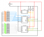
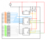
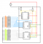
Quick and dirty wiring diagrams:

With 18M2 (works)
23882

With 08M2 (doesn't work)
23883

Program Code, same on both applications:
Code:
start:
    'init logic
    symbol RFRESH = C.0
    symbol SER = C.1
    symbol SRCLK = C.2
    symbol LBTN = C.3'reassign from C.3 to C.6 for testing on 18M2
    symbol RBTN = C.4
    symbol MBTN = C.5
    symbol LoopCount = b4
    
    LOW RFRESH
    LOW SRCLK
    LoopCount = 0
    
mainloop:
    DO WHILE LoopCount < 16
        gosub IncDisplay
        pause 1000
    LOOP
    DO WHILE LoopCount > 0 
        gosub DecDisplay
        pause 1000
    LOOP
goto mainloop
stop
IncDisplay:
    HIGH SER
    pause 100
    HIGH SRCLK
    pause 100
    LOW SRCLK
    inc LoopCount
return
DecDisplay:
    LOW SER
    pause 100
    HIGH SRCLK
    pause 100
    LOW SRCLK
    dec LoopCount
return
 

Attachments

Buzby

Senior Member
Hi,

Welcome to the forum.

As premelec says, you need decoupling capacitors. Without these you circuit may work unreliably.

Also, the SERIN pin ( C.5 on the 08M2 ) needs to be held low, otherwise the PICAXE will possibly reset and restart at random times.

However, I see you have allocated a symbol for C.5, it looks like it's for a button. If you intend to use C.5 on the 08M2 for this purpose you will instead need to include the DISCONNECT command at the beginning of your code. See Manual 2 page 61 and Manual 1 page 46.

Cheers,

Buzby
 
Last edited:

westaust55

Moderator
Since neither circuit shows the SerialIn pin held low with a resistor I suggest a full schematic AND a photo of both circuits.
Photo needs to be straight down on the circuit and clear enough to trace the wiring.
If on a circuit board as opposed to a breadboard then photo of both sides of both boards.
 

GenericEvilGenius

New Member
Thanks for the suggestions, since i'm an enthusiast I expected it might be something fairly remedial that I'm missing. I'll try these suggestions after work and let you know if it helps. Thanks again for the help and your patience.
 

GenericEvilGenius

New Member
Perfect! I wasn't aware that the serial in pin was constantly scanning for new input, that explains a lot. Pulling it to ground seems to have fixed everything. I'll also take your advice re: decoupling capacitors to heat too. Thanks for providing me a valuable teaching moment.
 

premelec

Senior Member
Great... that is why it is often suggested to leave the 2 input programming resistors in place... so many details... have fun...
 

inglewoodpete

Senior Member
Those are low value series resistors for the leds. How much current can the 74HC595 supply?
@GEGenius: That's what data sheets are for - get to know them:).

The 74HC595 can supply up to 35mA per output BUT the chip limit is 500mW.

However, if you are driving all 8 outputs at once: I = P/E, so 500mW / 5v = 100mA max per chip. Ie 12.5mA per output pin.

Edit: If you hadn't realised, your original 18M2 circuit worked by chance rather than good design too. You either need the programming circuit (two resistors with or without the programming socket as per manual 1) or just pulling the "Serial In" pin low with a resistor connected to the 0v supply rail.
 
Last edited:

AllyCat

Senior Member
Hi,
The 74HC595 can supply up to 35mA per output BUT the chip limit is 500mW.
The 35 mA is an "Absolute Maximum" rating, not a "guarantee" that the chip will actually deliver that current. The nominal output current appears to be only 6 mA per pin, so it will very probably be the chip that limits the output current rather than the 56 / 68 ohm resistors (which are indeed far too low to do anything "useful").

If the pin driver output stages of the '595 are actually acting as "switches" (i.e. with a low voltage drop), then the power dissipation should be very low, unless the load capacitance and/or the frequency are very high (MHz). So the 500 mW is very unlikely to be a limiting factor, particularly as the data sheet specifies that the total current in the supply and ground pins should be a maximum of about 75 mA (depending on which data sheet you read), e.g. if all outputs are driven high or low at the same time. I don't know if that current is "realistic" (in practice, some data sheet values are highly pessimistic), but it is intended to protect against the catastrophic (i.e "fatal") failure of a chip's bond wire burning out, like a fuse.

I don't know if the red and green colours of the LED symbols in the diagram are intended to indicate their actual colours (in which case the ratio of the resistor values is the wrong way around), but I would expect to use around 560 ohms in series with a red LED, perhaps 390 ohms for green and 220 ohms for blue / white.

Cheers, Alan.
 

thunderace7

New Member
I'm new to shift registers but trying to learn thanks to the link supplied by Technoman.
I understand that normally data is clocked in to the memory registers and then latched to the output registers. On this circuit the 2 clock lines are connected so it seems to me that it is trying to latch data that is changing and a race condition exists between the memory registers and the output registers. Am I mistaken? Is it normal practice to common both clock lines when used in a configuration like this?
Thanks.
 

AllyCat

Senior Member
Hi,

It's definitely envisaged because the (Texas) Data Sheet specifically says:

"Both the shift register clock (SRCLK) and storage register clock (RCLK) are positive-edge triggered. If both clocks are connected together, the shift register always is one clock pulse ahead of the storage register."

It's one of the reasons why a maximum risetime (slew rate) is often specified for clock waveforms, to rely on the propogation delays through the chip (although I didn't see anything in that specific data sheet). In practice, I believe the chips are designed with slightly differing clock threshold voltages, such that the "downstream" part of the system responds earlier (i.e. at a lower voltage) than the upstream clock, so it always "wins" the race. But your observation does highlight that care is needed in the design of clock driver circuits. ;)

A more rigorous solution, of course, is to invert one clock with respect to the other.

Cheers, Alan.
 
Top