Hi,
I am trying to make a 20x2 load a single frequency for a local oscillator.
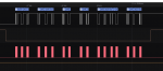
It appears to load, see logic capture below and the default freq shifts from 4.5GHz to 3.693GHz, but that falls short of the mark.
Question without notice, has anyone tried a 20x2 on a ADF534x?
'VK3GJM, 2021
'Sketch to load single Freq to ADF4351, cheap Chinese black PCB
#picaxe 20x2
#No_Table
#No_Data
hspisetup spimode00,spimedium 'sets High Speed SPI port
symbol LE = C.0 'pin 10 C.0 Latch Enable
symbol sck = B.7 'pin 11 B.7 hspi sck
symbol sdo = C.1 'pin 9 C.1 hspi sdo
'pin 13 B.5 hspi sdi, not used and tied to ground via 10K
InitADF: 'sets ADF4351 for 39410.7MHz using a 25MHz reference Frequency with a PFD frequency of 25MHz
high LE
pause 1000
low LE
'Write R0
hspiout (0x4e,0x03,0x58)
'Write R1
hspiout (0x80,0x08,0x7d,0x01)
'Write R2
hspiout (0x4e,0x42)
'Write R3
hspiout (0x4b,0x3)
'Write R4
hspiout (0x8c,0x80,0x3c)
'Write R5
hspiout (0x58,0x00,0x05)
high LE
Thank you
I am trying to make a 20x2 load a single frequency for a local oscillator.
It appears to load, see logic capture below and the default freq shifts from 4.5GHz to 3.693GHz, but that falls short of the mark.
Question without notice, has anyone tried a 20x2 on a ADF534x?
'VK3GJM, 2021
'Sketch to load single Freq to ADF4351, cheap Chinese black PCB
#picaxe 20x2
#No_Table
#No_Data
hspisetup spimode00,spimedium 'sets High Speed SPI port
symbol LE = C.0 'pin 10 C.0 Latch Enable
symbol sck = B.7 'pin 11 B.7 hspi sck
symbol sdo = C.1 'pin 9 C.1 hspi sdo
'pin 13 B.5 hspi sdi, not used and tied to ground via 10K
InitADF: 'sets ADF4351 for 39410.7MHz using a 25MHz reference Frequency with a PFD frequency of 25MHz
high LE
pause 1000
low LE
'Write R0
hspiout (0x4e,0x03,0x58)
'Write R1
hspiout (0x80,0x08,0x7d,0x01)
'Write R2
hspiout (0x4e,0x42)
'Write R3
hspiout (0x4b,0x3)
'Write R4
hspiout (0x8c,0x80,0x3c)
'Write R5
hspiout (0x58,0x00,0x05)
high LE
Thank you