74LS164 and seven-segment LED display

dusko

New Member
I am trying to extend picaxter's code for two seven-segment LED displays and
two 74LS164 from

http://www.picaxeforum.co.uk/showthread.php?t=7847&highlight=seven+segment+led+display&page=2

Instead of two displays (as in the original message), I'd want to use three displays and three 164's. I've tried many combinations of low 0, high 1 etc. inside shftout routine, but without any success. Obviously, I do not understand how the "serial in--parallel out" transfer works. I would appreciate very much if someone can show me the code for the shftout subroutine extended to three LED displays.
 

moxhamj

New Member
I'd start simple and work up. Use just one 164 for the moment and have a read of the data sheet http://pdf1.alldatasheet.net/datasheet-pdf/view/46131/SLS/HC164.html Write your own code to make the picaxe pins go high and low with long delays of several seconds so you can see and measure the pulses going into the shift register. Look at the Function Table in the data sheet to see what the lines need to be - you will see the data shifts on rising clock pulses. Once you get one working it becomes easy to daisy chain them and take out the delays.
 

Michael 2727

Senior Member
The CD4026 may be a better option, they are
a dedicated display driver rather than a shift
register chip.
You can drive 7-Seg Displays directly from the
CD4026 chip they are internally limited to 4mA
per Segment @ 5V.
If you need a very bright display you will need
a transistor drive for each Segment.
And they are cascadable like the other chips.

Two pins to work them, Reset and Pulse/Count.
 

picaxester

Senior Member
First you should try playing with the 74xx164 by it's self, with out the PICAXE.

Set up the 74xx164 with 1K resistors and LEDs running to ground on the outputs.
Tie the reset (clr) pin high. And of course supply power to the chip by running pin 7 to ground ( - ) and pin 14 to +5V (+4.5V or what ever).
Use 10k or 4.7k resistors to pull the clock and data pins low ( - ). From +v to the clock and data pins run 0.1uf caps (marked 104).
Add button switches across the two caps.
Now to test it. First press and hold the data button down then click the clock button a couple of times now release the data button and click the clock button a couple of times.

That should help you understand how to use them. And help you to make your own code if needed :)
 

dusko

New Member
Thank you to all who responded, especially to picaxester with the detailed description of the setup to learn how this works.

I can report that my project is working now. I thought that it was a software problem. However, after rebuilding my project on a new breadboard, everything worked as it should (my old breadboard had quite a few loose contacts). The only change I had to make to picaxester's code was

shftout:
for b1 = 0 to 7
low 0 'SCLK
low 1 changed this to high 1
if bit7 = 0 then Skiphigh
high 1 changed this to low 1
Skiphigh:
high 0 'SCLK
b0 = b0 * 2
next b1
return

since my LED displays are common cathode.

However, there are quite a few things that I still don't understand. I think I understand that PIN 0 (CLK) is a going high or low (I am not sure which) and then one bit of data (from b0) is being transfered to 164, to appear on one of the eight outputs. I don't understand the relation of bits in b0 and the transfer channel" between PIN1 (on PICAXE) and pins A and B (on 164). Also,
what is the role of b0 = b0 * 2 ? I understand that it shifts all bits leftwards, getting rid of MSB. The only guess I can make here that it somehow marks the end of a byte sent and eight "new" bits are expected.

Thanks again for all your help.
 

moxhamj

New Member
If you want to send out a high or low you need to do this at a certain point in time - eg a line might be going high and low so how does the 164 know when to read data. It does so when the clock signal changes so whenever it detects the low to high transition of the clock (as per the function table) it reads in whatever is in on the data line.

b0=b0*2 shifts the bits by 1 and it helps to understand binary. Eg 000 is 0, 001 is 1, 010 is 2 and 011 is 3 etc. Say you have 001 and you multiply it by 2 eg b0=b0*2 then in decimal that is 1*2=2 which in binary is 010. You can see the bit shifted over by one. Multiply 2*2=4 which in binary is 100 which again shifts by 1.
 

RickAlty

Senior Member
For seven-segment use, I think you can't beat the M5451. It lets you drive 5 seperate 7-segment delays using only two outputs from the PicAxe. For more than 5, you need only one more output for each set of five.

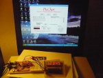
The picture below shows five digits being displayed from the output from the PC.

Richard
 

Attachments

profmason

Member
Another Option

I used a 74LS595 instead of the 74LS164. The 595 is the same as the 164 except it is latching. My writeup is at http://profmason.com/?p=151. I am still using a ULN2003 to sink the current for the 7 segment. You will need a separate driver and multiplexer for each segment. For a later project I used a 4026 as someone suggested earlier. The 4026 only needs two inputs for any number of segments. However, the control gets a bit tricky because you use the reset and clock pulse to set the digits. So a reset, followed by 127 pulses would display 127 on 3 leds. Here is a link to a stopwatch project I made using the 4026. http://profmason.com/?p=404
Even though it uses a 555 instead of a picaxe, it might be worth looking at.

good luck!
 

dusko

New Member
profmason,

Thank you very much for your help. Your pages are full of useful information. By going through your explanations about shift registers I think I finally understand how the serial in--parallel out transfer works.
 

RickAlty

Senior Member
RickAlty,
This looks very attractive. Can you please post more details (schematic/code)?
The datasheet for the M5451 chip can be found at

http://www.ortodoxism.ro/datasheets2/e/0zqj6og5wcoq8y1zyxt7r79056py.pdf

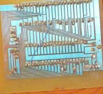
For some reason I can't find the pcb layout file so I just attached a photo of it. Here...

Code:
main:

	symbol clock=3
	symbol data_out = 4
	high clock
	pause 1
	low clock
	pause 1
	high data_out
	high clock
	pause 1
	low clock
	low data_out
	pause 1
	serin 1, n2400, #b1, #b2, #b3, #b4, #b5
	let b0=b1
	gosub test
	let b0=b2
	gosub test
	let b0=b3
	gosub test
	let b0=b4
	gosub test
	let b0=b5
	gosub test
	goto main

test:
	if b0=1 then one
	if b0=2 then two
	if b0=3 then three
	if b0=4 then four
	if b0=5 then five
	if b0=6 then six
	if b0=7 then seven
	if b0=8 then eight
	if b0=9 then nine
	if b0=0 then zero
	if b0="" then blank
	return

blank:

'pin 1
	pause 1
	high clock
	pause 1
	low clock
'pin 2
	pause 1
	high clock
	pause 1
	low clock
'pin 3
	pause 1
	high clock
	pause 1
	low clock
'pin 4
	pause 1
	high clock
	pause 1
	low clock
'pin 5
	pause 1
	high clock
	pause 1
	low clock
'pin 6
	pause 1
	high clock
	pause 1
	low clock
'pin 7
	pause 1
	high clock
	pause 1
	low clock
	return

one:

'pin 1
	pause 1
	high data_out
	high clock
	pause 1
	low clock
	low data_out
'pin 2
	pause 1
	high clock
	pause 1
	low clock
'pin 3
	pause 1
	high clock
	pause 1
	low clock
'pin 4
	pause 1
	high clock
	pause 1
	low clock
'pin 5
	pause 1
	high data_out
	high clock
	pause 1
	low clock
	low data_out
'pin 6
	pause 1
	high clock
	pause 1
	low clock
'pin 7
	pause 1
	high clock
	pause 1
	low clock
	return

two:

'pin 1
	pause 1
	high clock
	pause 1
	low clock
'pin 2
	pause 1
	high data_out
	high clock
	pause 1
	low clock
	low data_out
'pin 3
	pause 1
	high clock
	pause 1
	low clock
'pin 4
	pause 1
	high clock
	pause 1
	low clock
'pin 5
	pause 1
	high clock
	pause 1
	low clock
'pin 6
	pause 1
	high clock
	pause 1
	low clock
'pin 7
	pause 1
	high clock
	pause 1
	low clock
	return

three:

'pin 1
	pause 1
	high clock
	pause 1
	low clock
'pin 2
	pause 1
	high clock
	pause 1
	low clock
'pin 3
	pause 1
	high data_out
	high clock
	pause 1
	low clock
	low data_out
'pin 4
	pause 1
	high clock
	pause 1
	low clock
'pin 5
	pause 1
	high clock
	pause 1
	low clock
'pin 6
	pause 1
	high clock
	pause 1
	low clock
'pin 7
	pause 1
	high clock
	pause 1
	low clock
	return

four:

'pin 1
	pause 1
	high clock
	pause 1
	low clock
'pin 2
	pause 1
	high clock
	pause 1
	low clock
'pin 3
	pause 1
	high clock
	pause 1
	low clock
'pin 4
	pause 1
	high data_out
	high clock
	pause 1
	low clock
	low data_out
'pin 5
	pause 1
	high clock
	pause 1
	low clock
'pin 6
	pause 1
	high clock
	pause 1
	low clock
'pin 7
	pause 1
	high clock
	pause 1
	low clock
	return
	
five:
	
'pin 1
	pause 1
	high clock
	pause 1
	low clock
'pin 2
	pause 1
	high clock
	pause 1
	low clock
'pin 3
	pause 1
	high clock
	pause 1
	low clock
'pin 4
	pause 1
	high clock
	pause 1
	low clock
'pin 5
	pause 1
	high data_out
	high clock
	pause 1
	low clock
	low data_out
'pin 6
	pause 1
	high clock
	pause 1
	low clock
'pin 7
	pause 1
	high clock
	pause 1
	low clock
	return
	
six:

'pin 1
	pause 1
	high clock
	pause 1
	low clock
'pin 2
	pause 1
	high clock
	pause 1
	low clock
'pin 3
	pause 1
	high clock
	pause 1
	low clock
'pin 4
	pause 1
	high clock
	pause 1
	low clock
'pin 5
	pause 1
	high clock
	pause 1
	low clock
'pin 6
	pause 1
	high data_out
	high clock
	pause 1
	low clock
	low data_out
'pin 7
	pause 1
	high clock
	pause 1
	low clock
	return
	
seven:

'pin 1
	pause 1
	high clock
	pause 1
	low clock
'pin 2
	pause 1
	high clock
	pause 1
	low clock
'pin 3
	pause 1
	high clock
	pause 1
	low clock
'pin 4
	pause 1
	high clock
	pause 1
	low clock
'pin 5
	pause 1
	high clock
	pause 1
	low clock
'pin 6
	pause 1
	high clock
	pause 1
	low clock
'pin 7
	pause 1
	high data_out
	high clock
	pause 1
	low clock
	low data_out
	return
	
eight:

'pin 1
	pause 1
	high clock
	pause 1
	low clock
'pin 2
	pause 1
	high clock
	pause 1
	low clock
'pin 3
	pause 1
	high clock
	pause 1
	low clock
'pin 4
	pause 1
	high clock
	pause 1
	low clock
'pin 5
	pause 1
	high clock
	pause 1
	low clock
'pin 6
	pause 1
	high clock
	pause 1
	low clock
'pin 7
	pause 1
	high clock
	pause 1
	low clock
	return
	
nine:

'pin 1
	pause 1
	high clock
	pause 1
	low clock
'pin 2
	pause 1
	high clock
	pause 1
	low clock
'pin 3
	pause 1
	high clock
	pause 1
	low clock
'pin 4
	pause 1
	high clock
	pause 1
	low clock
'pin 5
	pause 1
	high clock
	pause 1
	low clock
'pin 6
	pause 1
	high clock
	pause 1
	low clock
'pin 7
	pause 1
	high clock
	pause 1
	low clock
	return
	
zero:

'pin 1
	pause 1
	high clock
	pause 1
	low clock
'pin 2
	pause 1
	high clock
	pause 1
	low clock
'pin 3
	pause 1
	high clock
	pause 1
	low clock
'pin 4
	pause 1
	high clock
	pause 1
	low clock
'pin 5
	pause 1
	high clock
	pause 1
	low clock
'pin 6
	pause 1
	high clock
	pause 1
	low clock
'pin 7
	pause 1
	high clock
	pause 1
	low clock
	return

end
is the code that runs the five digits. The downside to a chip like this is that you have to display the digits 'segment by segment'.

The application PicChat, for the person who asked, I wrote myself to test the interface between the PC and the PicAxe. It lets you use the slider to move a servo, or send data for a stepper or LEDs etc, and read the outputs back from the PicAxe.

I put the program up on this forum a while ago, but if anyone else wants it just let me know.

Richard
 

Attachments

boriz

Senior Member
@RickAlty
What language?. Did you use an IO DLL?. How? Can I see your source?

For a while now, I have been thinking about writing a small PC IO app for a PICAXE using Emergence BASIC (http://www.ionicwind.com/).

Not yet gotten around to it. Any tips?
 
Top