3 digit display using 74HC595

westaust55

Moderator
From time to time the need for more outputs or a means of driving displays etc arise.

One method is to use several 74HC595 shift registers with latching tri-state outputs. The latching outputs has the advantage that the outputs are not disturbed (and nor is the driven device) while the new data is being shifted into the shift registers.

The next few posts present:
1. PEBBLE board layouts (this post)
2. Schematic diagram
3. Photos of the two boards created
4. Photos of the display in operation
5. Programs for smaller (08M) and larger PICAXE chips


EDIT: 15Apr2012 The layout image for the 74HC595 shift register Board has been corrected.
 

Attachments

Last edited:

westaust55

Moderator
Here is the schematic diagram.

Note that for flexibility, the Output Enable (OE) has a pull-down resistor while the shift register clear (SRCLR) has a pull up resistor.
As such, the board will function correctly with no PICAXE control of these signals but for larger PICAXE chips, it is possible to also control these two lines as desired.

This allows smaller PICAXE such as the 08M to be used with just 3 outputs but larger PICAXE chips with more outputs available can use up to 5 control lines if desired.
 

Attachments

Last edited:

gengis

New Member
Thank You westaust55

I was trying to figure out how to get an M08 to play a full octave of chimes.
 

westaust55

Moderator
Note that the program example for smaller PICAXE chips (ie with title including "-suit 08M") for the newer M2 parts the label "ShiftOut" is apparently a reserved word. Therefore in the program change all instances for "ShiftOut" to say "ShiftoutM2".

The second version will compile correctly for X1 and X2 parts.
 

mrburnette

Senior Member
Absolutely wonderful to have a fully documented 3-digit board and associated PICAXE code. Perhaps you could go back and annotate to VIAD2 this thread reference for his 120 second count down clock. My push toward using the AXE133 OLED was simply to be able to simplify the code to SEROUT so that he felt comfortable and was able to process the countdown in the simulator as the frustration level was beginning to appear. When working with something other than blinking LEDs, it surely is helpful to have a generic PICAXE project as the starting-point for discussion.

Brilliant.

- Ray
 

westaust55

Moderator
Hi Ray,

Thanks for the compilment.

While there are certainly many other ways (multiplexing, use of dedicated BDC to 7-Segment chips such as CD4026, etc) to drive some 7-Segment displays,
the intent here was as much to show how to use some 74HC595 shift registers in cascade to gain many outputs controlled from just 3 PICAXE output pins.
The 74HC595 was frequently referenced in the past on this forum with newcomers struggling with some aspects such as cascading but the '595 seems to have fallen out of favour
with few references in recent times.

Combined with some cascaded 74HC165 Parallel to serial shift registers for inputs, you could expand an 08M or 08M2 to many Ipnuts and Outputs with just 4 or 5 IO required.
With the newer M2 parts having i2c comms inbuilt, use of such chips as the MCP23017 provides 16 bi-directional IO as two 8-bit ports per chip.
 

Blue Beta

New Member
wonderful piece of work here but i'll be honest im now more confused than before i read it.
i came here from the following page and my question is regarding the Three 74HC575 to three 7-seg dispays for larger PICAXE.bas

http://www.picaxeforum.co.uk/showthread.php?20412-Help-!-PICAXE-08M2-with-a-74HC595-Shift-Register-and-Im-a-total-noob

regarding the "lookup" command - would i be right in thinking you've abbreviated the eight ones and zeros required for the shift register in hexadecimal?
if so how exactly did you separate out the highs and lows so you could send the other signal required by the shift to move it along?

its probably a straight forward answer but please remember im completely new to this and learning off bits i pick up off the net

thanks

dominic

btw - i'm posting the same question on lets make robots - hope you dont mind but i know more people there (and frankly the more versions i get the more likely i am to actually understand one)
 

westaust55

Moderator
Welcome to the PICAXE forum.

If you look at the schematic you will see that I did not use a more conventional allocation of the LED segments to the byte bit values.
When you are using a lookup table it can be far easier to make the wiring side easy and adjust the bit to segment allocations in the lookup table and avoid many crossing wires.

The attached diagram will hopefully help you understand hope the bit to segment allocation was done for my project. Also how the byte values can be in hexadecimal or binary where the individual bits are shown.
 

Attachments

Blue Beta

New Member
hi west - thanks for the reply

I'll be honest segment allocation was the least of my problems - but it will be useful to know when i start to get into the nitty gritty.

i'm more confused by how you take a whole number in hex - convert it to binary and then separate out the different ones and zero's so that you can send them individually to the shift register - i'm thinking out loud but the equivalent would be divide a decimal number by ten, round it down to the nearest whole number and subtract that from the original - thus 47 would give you a separate 4 then a 7. can you do that in binary?

my biggest problem is im working off a small group of commands and no actual training in how to use them.

I'll leave it there for now but trust me when i say i have a serious number of questions so there's a good chance I'll become an annoying regular on here ;)

dom

looking around - something tells me shiftout and mask are going to be involved and life looks like its about to get very complicated.
 
Last edited:

techElder

Well-known member
Blue Beta, always work backwards.

Look at what the display needs to light each segment. That will be a group of 1's and 0's (depending on common anode or common cathode or sink or source). Eight of those 1's and 0's becomes a byte. You know that a certain pattern of those 1's and 0's lights up a particular pattern on the display; perhaps it is the number "8".

You know now that you have to send that byte to make the display show an "8".

So, when your program needs an "8" to be displayed, you send that pattern of 1's and 0's (a byte) to the 74HC575.

You can send it as a pattern of 1's and 0's (binary) or convert it to HEX or even DECIMAL. The same pattern of 1's and 0's are sent.

Work backwards from what your display needs back to what you have to send it.
 

westaust55

Moderator
The value in a byte variable is always stored by the PICAXE microcontroller in binary format irrespective of whether you define the value in binary, hexadecimal or decimal.
With the binary format there are always 8 bits where the least significant bit (or bit 0) is by industry convention depicted on the right side through to the most significant bit ( or bit 7) which is depicted on the left hand side.

With the X1 and X2 PICAXE chips there are inbuilt commands (SHIFTOUT) to serially send the data to the external shift registers (eg 74HC595) including control of the clocking signal.

With the other PICAXE chips such as the 18X, M parts and newer M2 parts you need to use your own small subroutine. If you look in PICAXE manual 2 udner the SHIFTOUT command examples of the small routines to extract each bit and send out to the shift register with the necessary clocking signal line are provided.
As each bit is shifted out, the remaining bits are shifted along so that the program only looks at one bit position to determine the level ( 1 or 0) to be set on the data output line before the clock pin is pulsed.
 

TAMeyer

Member
This is a helpful tutorial and using your code, I was able to simulate using a single 08M and three separate 595s driving three 7 segment LEDs in VSM. This is encouraging as flicker has been an issue with multiplexing.

Thank You.

The problem I cannot solve is how to wire and code for multiple 7-segment displays (CC) encased in a single package. The anode leads are shared, so “crosstalk” between digits is a problem.

90% of my display inventory is these types of multiple sets, yet single 7 segment displays can be had for almost nothing, so this is an academic discussion.

In post 10 you comment that the intent was designed to show how shift registers can be used to an advantage. 7-segments displays are a common ground for many and a visual goes a long way in presenting an idea.

I am a novice, and can barely hang on to many of the advanced discussions on the forum.
But in writing this post it occurs to me that;

I answered my own question?
For multiple displays sharing common leads, other solutions may be more expedient?

True?

There's always the 7219........$$$


The attached is one of many attempts at solving the issue.

Thanks in advance,

Terry


Code:
; ====================================================================
;   File....... Three 74HC575 to three 7-seg dispays for 28X1 or 40X1
;   Purpose.... Program to use three cascaded 74HC595 shift registers
;            to drive three 7-segment displays
;   Author..... Westaust55
;   E-mail.....
;   Started.... 24-10-2009
;   Updated.... DD-MM-YYYY
;  ===============================================
;
; -----[ Program Description ]---------------------------------------------
;
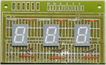
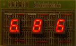
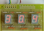
; A program to drive three 74HC575 to three 7-seg dispays and diplays values
; on three 7-segment displays to show the values  from 0.00 thru 0.01 ... to 999.
; 
;
; -----[ Revision History ]------------------------------------------------
; A. First written 24-10-2009
; B. Added Out Enabled pins for three 7 segment LEDs manufactured in a single package with shared leads
; 
;
; -----[ I/O Definitions ]-------------------------------------------------
;
; - - - DIGITAL INPUT PINS  - - -
;
; - - - DIGITAL OUTPUT PINS - - -
;
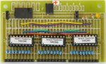
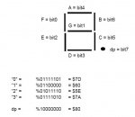
SYMBOL RegCl   = 3    ; Shift Register Clear - Low to clear
SYMBOL OutEn2  = 2     ; Output Enable Digit2 (far left). Low to enable 100s Outputs
SYMBOL OutEn1  = 1     ; Output Enable Digit1 (ctr) Low to enable 10s Outputs
SYMBOL OutEn0  = 0     ; Output Enable Digit0 (far right) Low to enable units Outputs
SYMBOL latch   = 5    ; latch data to 595 outputs
SYMBOL sclk    = 6    ;  serial clock on pin 6
SYMBOL sdata   = 7    ; serial data on pin 7


;
; - - - ANALOGUE INPUT PINS  - - -
;
;
; -----[ i2c Device Addressing ]-------------------------------------------------------
;


;
; -----[ Constants ]-------------------------------------------------------
;
;
;
; -----[ Variables ]-------------------------------------------------------
;
; define aliases names for variables used
SYMBOL bitcntr = b3     ; control for serial shifting of data out
SYMBOL digit   = b4    ; extracted digit from 3 digit value 0 - 999
SYMBOL digout  = b5     ;  encoded value 7-seg display  to the output with serial shifting
SYMBOL mask    = b6     ;
SYMBOL decpnt  = b7
; 
; -----[ EEPROM Data ]-----------------------------------------------------
;
;
;
; -----[ Initialization ]--------------------------------------------------
;


Init:  
disconnect
      Low sclk    ; make sure the clock and data lines are low in advance
    Low sdata
      ' Low OutEn    ; Enable the 74HC595 outputs
      High RegCl    ; Remove the 74HC595 clear signal
     decpnt = 0
;        
SetFreq k31


; -----[ Program Code ]----------------------------------------------------
;
 
Main:
    FOR b2 = 1 TO 3 ; three decades to display  0.00 to 9.99, 00.0 to 99.9 and 000. to 999.
        FOR w0 = 0 to 999 ; range of the display
        
        ; Demonstrate use of Output Enable and Clear Signals if count between 500 and 550
            IF w0 > 500 AND w0 < 550 THEN
                If b2 = 1 THEN        ; First cycle disable outputs so no display
                    High OutEn0
                    High OutEn1
                    High OutEn2
                ELSEIF b2 = 2 THEN    ; Second cycle clear the shift registers
                    Low RegCl        ; again the 7-seg displays are all off
                ENDIF
            ENDIF
            IF w0 = 551 THEN            ; restore at end of the "feature"demo period
    '            LOW OutEn0
    '            LOW OutEn1
    '            LOW OutEn2
                HIGH RegCl
            ENDIF
        
        ; Normal count and display portion of the code
            
            digit = w0 // 10 ; extract units digit
            IF b2 = 3 THEN 
                decpnt = 1  
            ENDIF
            LOW OutEn0
            GOSUB ShiftoutMSBFirst ; fetch the bit code for the current digit value and shift out
              High OutEn0
          
            digit = w0 // 100 / 10  ; extract the tens digit
            IF b2 = 2 THEN
                decpnt = 1   
            ENDIF
            LOW OutEn1
            GOSUB ShiftoutMSBFirst
            High OutEn1
            
            digit = w0 / 100   ; extract the hundreds digit
            IF b2 = 1 THEN
                decpnt = 1   
            ENDIF
            LOW OutEn2
            GOSUB ShiftoutMSBFirst
            High OutEn2
            pulsout latch,5 


        NEXT w0
    NEXT b2
    GOTO Main        ; loop through the values 0.00 to 999 forever


           END
;
; -----[ Subroutines ]-----------------------------------------------------
;
ShiftoutMSBfirst:
; First find the display code for 7-seg display corresponding to the digit value 0 -9
'    LOOKUP digit, ($7D,$60,$5E,$7A,$63,$3B,$3F,$70,$7F,$7B), digout ; change $70 to $56 for different "7" appearance
    
    LOOKUP digit, ($3F,$06,$5B,$4F,$66,$6D,$7D,$07,$7F,$67), digout
    ; change $70 to $56 for different "7" appearance


    IF decpnt = 1 THEN
        digout = digout OR $80 ; turn on bit 7 for decimal point
        decpnt = 0
    ENDIF
;
; Then shift data out serially - most significant bit first
    FOR  bitcntr = 1 TO 8  ; one loop per bit
        mask = digout  & $80 ; Mask out the MSB 
        LOW sdata
        IF mask = 0 THEN skipMSB
        HIGH sdata
skipMSB:     pulsout sclk,1    ; pulse clock line for 10us
        digout = digout * 2    ; shift value left ready for next bit


    NEXT bitcntr
RETURN
;
;
;
; -----[ Interrupt Routines (if used) ]-------------------------------------
;
;Interrupt: 


;           RETURN
; =================================================
;      THE END
; =================================================
 

Attachments

Top